Revisiting the Counterfeit ATMega328s
A SparkFun customer and a a local dentist investigate the ATMega328 "slugs" - with interesting findings.

We made a post about the ATmega328 Slugs a little while back. The short version of the story is that we got some ATmegas that we couldn't get working. Are they counterfeit or are we inept at getting a microcontroller running? Hmmm.

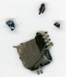
A functioning ATMega on the left with a fake one on the right.
Ignoring the obvious questions of why the supplier bothered sending us anything or went through the hassle of creating parts that looked like the real things in some ways (packaged and stamped) but not in others (incorrect numbers and, um, they don't work...), we were a bit intrigued by what was actually inside these parts.

Our initial tests revealed what appeared to be just copper - certainly no silicon.
Our early investigation was fairly fruitless. After spending a couple hours running the problem ICs through an acid bath, we found nothing but metal inside. But perhaps we etched the entire IC away, or not enough, we're not sure (that's part of the joy of trying something random and new!). Fortunately, a SparkFun customer took it upon himself to do his own testing - which revealed some very interesting details.

Wait...silicon? Really?
So it's not just molded plastic injected with copper of some kind? It appears there is actually silicon and gold wire bonds in there. Check out the WTF Moogle blog to find out more about what he found.
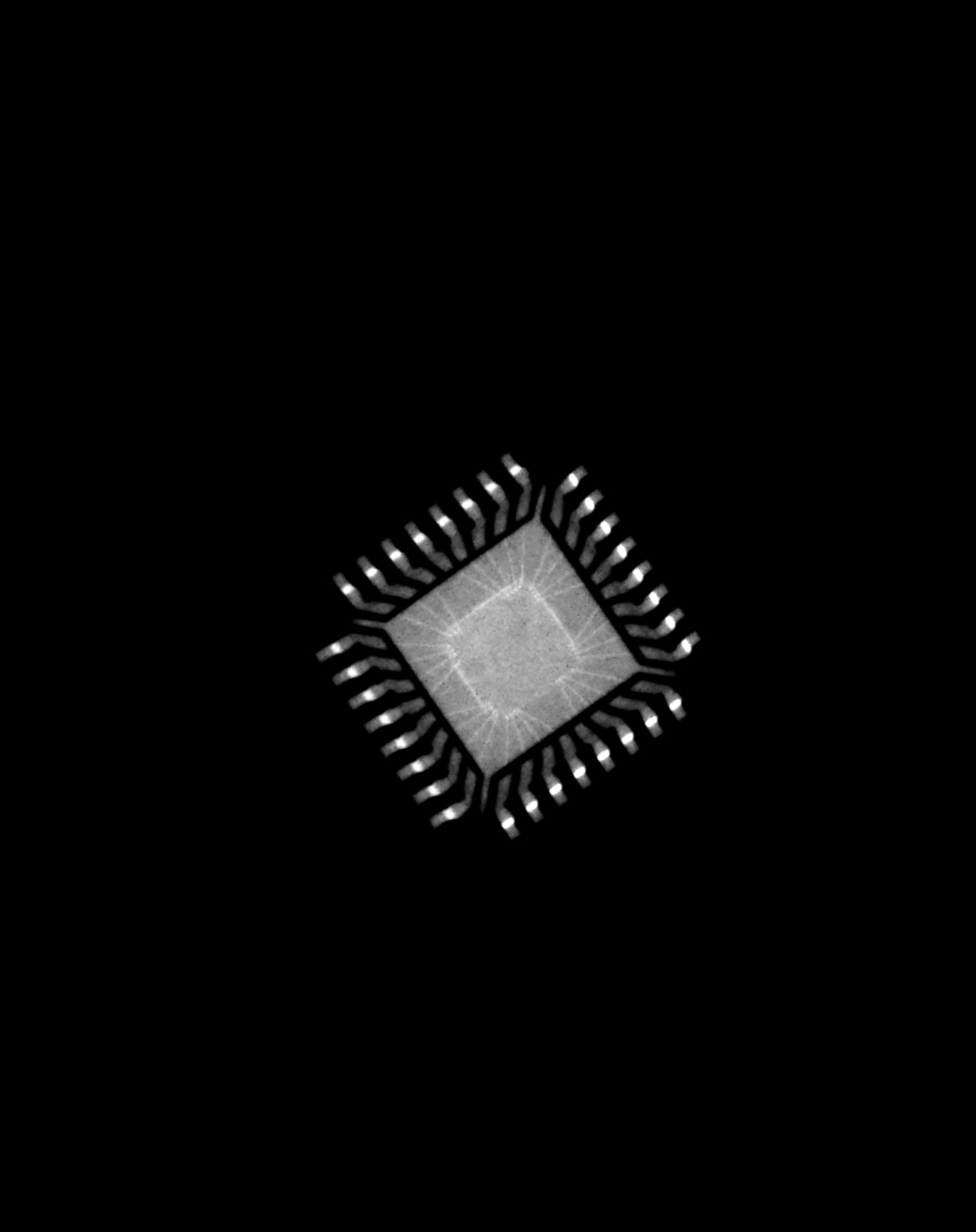
This is what an x-ray of a real ATMega328 looks like.
We also did a little more investigating of our own. Lindsay (our Assistant Production Manager, ex-chemist, and is generally friends with people who have access to awesome tools!) took the ICs to her friend who is a dentist and x-rayed both. What do you see?
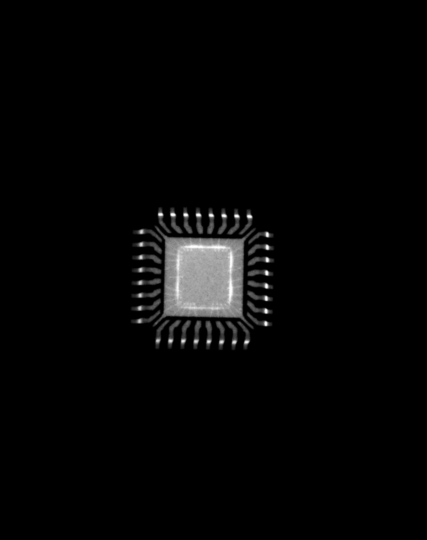
This is the x-ray of the counterfeit ATMega - clearly it's not just solid copper.
There is definitely something going on in the fake - it looks remarkably like the real one. So what's the deal here? The mystery continues.
Be sure to read the original post, the follow up report, the discovery of what's inside and the final identification of the IC!


Why not give them out as conciliation prizes for anyone that didn?t get their $100 freebies in January?
If yours works you get a $1000 spree. Never mind? since it?s a sucker bet make it a $1E6 spree.
Hmm. Maybe if you sell enough of the slugs you can use the proceeds to pay for professional decapsulation and get a good look at the die. Searching for "IC decapsulation" will get you some leads to failure analysis houses that do this for a living. Runs $150-250 IIRC.
Looking at the document revisions at the end of the ATMEGA328P datasheet, the first revision was in 7/2007 - considerably earlier than the sept 2008 first chip availability seen in the previous post, but still well beyond the 23rd week of 2007...
http://www.atmel.com/dyn/resources/prod_documents/8025s.pdf
And they always seem to have datasheets available well before the chips are, so as said before, that date code is extremely unlikely to be legitimate. And looking at the original rev of the datasheet (i dug it up: http://www.datasheetpro.com/971197_download_8025A_datasheet.html ) I don't see anything that says they don't work!
That makes me seriously doubt these are anything other than fancy counterfeits. As someone said, they probably had other blank chips and just screened them with something expensive.
-Taylor
Fuming nitric works better to eat away that package. Also, the Xray pretty much showed the wirebonding/pads - so you know it's not just a Cu slug. I would suggest saw/polish the die in half, then look under a microscope and see if you can spot the interconnects within the die. By the Xray, the pads are in a different orientation on the counterfeit. I'm guessing these are counterfeit, but pretty good ones. If you have access to FIB/DIB and SEM you could image some of the exposed silicon. Perhaps do some polish to get into the traces first?
And you havent tried to talk to anyone at atmel? it seems like they would want to know if someone is making fake chips and im pretty sure they could tell you if it was an early version or just not theirs..
haha i fail to read
Have you contacted Atmel about these? I'm pretty sure they'd want to pursue any counterfeit chips claiming their name, and they'd have all the big toys to analyze them.
So, from what I understand, it's pretty common for shady asian "chip companies" to just find old circuit boards, iron the chips off, and re-silk screen new labels on them and sell them back to us as if they were new chips... Sometimes they just change part of the label so it appears to be a higher quality part than it actually is, sometimes they put something completely different on there that just looks the same.
I'm guessing it's just another chip made by atmel (maybe even an mcu), where they just changed the main title so you'd think it was an atmega and not the part it actually is. It probably has the fuses set to disable programming because it was already deployed once in a production project.
I'm curious. I know it is a shot in the dark and there are MANY chips manufactured in that package, but considering the size of the die, I'm wondering if these are not Parallax' Propeller microcontrollers?
I remember Chip Gracey (who created the Propeller) mentioning how the die takes up almost the entire package. Again, shot in the dark, but if the Propeller and ATMega are manufactured at the same facility...
The Parallax Propeller has 11 pins per side. These ATMega chips have 8 pins per side. (I use the Propeller a lot. I think it is a great chip.)
Are there any of these fake ATMegas left? I wouldn't mind getting my hands on a few to see a bit closer what's inside.
http://oms.wmhost.com/misc/reminder.jpg
The die size is way bigger on the counterfeit, it could be old parts from before a "die shrink", if it's a ATMega328 at all. The factory reject dies could have been packaged by someone.
I just took a course offered by JPL on counterfeit parts. I was amazed at all the ways thugs and crooks doctor chips to make them look like the real deal.
the chip on the left was made the 4th week of this year and the one on the right was made the 23 week of '07.
if it is a real Atmel chip then it is certainly an older
batch. Check out this video if you want a real taste of what an earlier poster was talking about:
http://www.pbs.org/frontlineworld/stories/ghana804/video/video_index.html
Very interesting video. Thank you for sharing this with the community. This is something that we all need to be aware of. Electronic waste is a terrible side effect to the electronic revolution.
Have a look at this article: http://www.bunniestudios.com/blog/?p=918
In that case it was SD card instead of AVR. If you read his story (he has on the ground experience in China) it look slike the same fab house assembly lines are used to produce these counterfeit chips only with cheap materials.
I am an engineer and have worked on several ASIC's. The copper slug is part of the leadframe, but the backside of the die attaches to the slug. The purpose is to get a solid Vss (or Vdd, depending on the process) connection to the die substrate. The pads where the bond wires attach is on the surface of the die, opposite the backside. Someone mentioned a bond wire that goes "nowhere" on the counterfeit -- that is how Vss (or Vdd) is connected to the copper slug from a Vss (or Vdd) trace on the topside of the die.
Semiconductor devices are first tested at the wafer level. Bad die are marked with an ink dot. The tested wafers are sent to a packaging house where the wafers are sawed into individual die. The die are packaged and then retested. Good packaged parts are then marked. These counterfeit parts are probably packaged parts that failed testing after packaging. These parts should be disposed of, but not all are. These parts just need to be marked to look "real".
Jeff
My guess is that the copper was to thermally enhance whatever was in the package. I doubt it is the "real deal". Of course, why not just decap the part and look under a microscope. The atmel logo, copyright, and the die identification will be in the silicon.
It is a real part of some type, so I don't think doing a contact or leakage test would yield much other than potentially identifying which pins are grounds.
Working for the company that I do we deal with this a lot especially since we deal with obsolete components. We had a presentation on the counterfeiting problem and they had a team that went to china and took photos of the counterfeiting operations. Basically what happens is all the E-waste gets shipped over to china. There is a specific town (don?t remember the name) that it?s pretty much all they do. They take all the components off of the PCBs and sort them by packages (DIP, SOT-23, QFP ect). They then sand/etch down all the markings. Next they give it to a guy that has a list of wanted parts and he marks them. It?s amazingly low tech the whole thing is. So basically you don?t have a clue as to what is in the package could be anything. It was interesting seeing all the pictures of people in the streets stripping down PCBs over a fire barrel. Real scary stuff, sadly most of them will have health complications from doing this but it?s the only way to make a buck there.
http://www.time.com/time/photogallery/0,29307,1870162,00.html
Nice. Copy and paste the whole link to get it to work.
It seems as though there is an extra wire bonded to the die in the counterfeit. On the left side in your picture, right in the middle. It doesn't seem to connect to anything. That might have a little something to do with it. Also, the dies are different sizes.
The copper layer could be for thermal dissipation and also for electrical noise suppression. In that case it might be where the extra wire attaches.
Look at old ceramic uP's and you'll find a grounded gold coating on top of a lot of the chips.
I just want to add my two cents.
I am a computer engineer with some knowledge in wafer production (just from the latest techniques and theory from former EEs at Intel, but nothing to extravagant). The biggest piece of evidence here is the X-rays. Looking at the legit version of the ATMega, you can see the wires running from the interior of the chip to the pins are very precise going to the center of the pins are are mils on the inside of the border of the chip itself. They are also grouped near the corners to reduce propagation delay and increase efficiency in floor print layouts.
The counterfeit shows lackluster shielding from the interior of the chip, and the lines are not (understatement) as precise as the legit. So if anyone is going to try and connect anything to it, a high probability dictates that it's just going to sink current/voltage/power to it. Not to mention the pins look oxidized, which is not how an IC should come.
I don't know, if anyone can fill me in on latest MCU production wafer techniques, that would definitely help out. Mainly because those wires connecting the interior to the pins is key here.
I want to stick one of these guys in an SEM! I would be glad to image over the entire chip and then tile them together to get one nice map. Sparkfun guys drop me an email.
Did you guys decide that you aren't going to sell any more of the slugs? I was hoping you were just taking a break to investigate the legalities and liabilities. I really like the idea of making a d6 out of them.
If it is a fuse issue this tastey piece of kit featured on HaD might help http://hackaday.com/2010/05/17/magically-repair-avr-chips/
A dentist xray machine is usually pretty crap. Fine for having a look at teeth surrounded by soft tissue but not much help seeing through a copper block. Try a CT :)
the real mystery to me would be when the hell will the real ones be available.
Interesting to see that counterfeits reached SparkFun! We develop x-ray systems for counterfeit detection. We've seen all kinds of weird stuff out there. We actually have quite a library of counterfeit parts that we use for training. As an old customer, I'd like to offer some help. Nate, would you like us to send you an x-ray system for you guys to play with? You'd be surprised what you are going to find out!
Something interesting is that the slug ATmega looks like the little wires leading to the pins are a whole lot less organized. Also, has anyone tried hooking up a (supposed to be) "power pin" of one of the slugs up as well as ground, and seeing if any other "GND" pins still read at a zero volt ref? Another idea is hook up power to the real one, measure values of resistance capacitance etc across known pins, and then see if the slug when hooked up to power has the same readings. It would also be nice to see xrays of similar form factor logic or PIC chips, to see if the inner pin wiring matches up to another known chip. Maybe they are a different mark ATMEL AVR or something...I don't know, and I don't have any to test on, which is why I am suggesting such a multitude of solutions. Hope this can be of help.
I work for a company, who will remain anonymous that manufactures e-beam lithography, FIBs, and chip scanning equipment. I would be very interested in looking at some of these if you guys could strip off the surface.
Hmm---curioser and curioser. I may have to buy a few fakes now. I work in the medical field, and have access to various types of x-ray imaging equipment, including megavoltage (as opposed to kilovoltage, like most diagnostic x-ray equipment) imaging equipment. Could be interesting to see how much detail I can get. If I can get enough detail to image the actual die....
Looking at the x-ray pictures, it is clear that the chips are not the same, the pad pitch on the ATMega is tighter, maybe suggesting smaller geometries, the counterfeit is a bigger die with more space between the pads, maybe a fail intent to reverse engineer the ATMega using an older process?.
I am glad that the xray/dentist suggestion worked for you guys, however, checking for continuity of input protect diodes may shine additional light on the issue of empty packages vs. real ones without need of ionizing radiation, just a dmm....
I thought about this. Silicon dies/wafer layout certainly changes over time with revisions so it is not unheard of that the wire bond pads on the die would have moved, gotten closer together, different wire bonding facility, etc. I'm really grasping at straws here, but it's possible.
Assuming they are indeed fake parts, then no reason to assume that all the chips look the same inside.
The chips could be anything really. Whats stopping them from grabbing any old run of ICs in that package and etching new fake numbers on them. Some kid could have found a few thousand tossed in a dumpster outside a china fab house that didn't get stamped then pay his cousin to sneak in and stamp them like the chips he makes every day anyway.
They are probably something bonafide that failed production, intercepted on their way to the trash, and then 'somehow' found their way to the imprinting machine..
I know this may be a bit of a stretch, but has anyone tried hooking up the pins backwards? Like when you flip a silk screen by accident and it looks like a mirror image? Maybe the pin outs are the same way.
@TheMoogle - Thanks for putting a second set of eyes on these! Now can you light up one of the duds you picked up? We couldn't get one to fire. This means either there's something really weird with the 0723 ATmega328s, or the silicon inside the IC is something completely wacky and it's just a relabel.
I would either contact the seller, maybe they were sold failed chips as someone else had said (failed final packaged test).
I know that every MCU is tested at wafer level, binned, and sold accordingly. To save costs, the bad die are rarely inked anymore, just virtually marked in a bin report, sent to the package house.
Are there numbers on the bottom of the chips which are bad? I have an ATMEGA32-16PC on my desk, with a date code of 0419 on the top, and 3N0697-1-355P6B 3N0416 stampped on the bottom. The numbers on the bottom have special meaning.
Atmel FA (failure analysis) may be interested in a few pieces. They can de-cap them and look at any product IDs on the die. They are in Colorado Springs. I am sure they would be interested in any counterfit leads....
I have the mailing address for some people there who can get a chip or two to where they need to go.
I have getto rigged one up to try and program one but I couldn't get any response from the chip.
It was acting like the fuses were set to disable programming. Maybe a HV programmer will work ?