
A little while back, we posted the video below that shows you how to do your own solder stenciling. If you're not familiar, solder stenciling is the process of using stencils and solder paste to connect components to your PCB quickly and easily. We feel like the video below does a pretty decent job of guiding you through the basics. But as we all know, nothing beats hands-on experience.
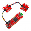
That is why we have added two new dates for our solder stenciling classes - July 14th and November 17th. Yes, these dates are pretty far out in the future right now, but we wanted to give you a heads-up in case you want to plan a trip to Colorado and take a solder stenciling class! In these classes, we'll show you the tools and techniques of the trade as you work on soldering a panel of Arduino Pros (one of which, you'll take home with you).
Look at all those tiny components you'll solder in minutes!
Solder stenciling is an awesome skill to have and something that we use heavily here at SparkFun. If you want to learn, these classes will give you all the tools you need. As always, keep an eye on our classes section for any new classes. Happy Monday, everyone!

How over/undersized do you guys make the holes in the stencil to get the best results?
Inquiring minds would like to know... Thanks!
However, with that said, I do make numerous assembly specific modifications depending on process results. For example, the manufacturer of a microBGA recommended 10mil round apertures for the component, but after poor results, I ended up going with a 12.5 mil rounded corner square aperture.
There is some geometry, physics, and a bit of magic involved with stencils when dealing with complex assemblies.
It's all about proper paste volume. For 2-4mil thick mylar stencils, 1:1 is typical because of paste volume. Not sure about Sparkfun's setups, but here are some industry standard mods for 5 and 6 mil stainless steel stencils:
For tin/lead chemistry, most stencil apertures are reduced 10%. Some fine pitch parts will have the length of the pads left at 100% to maintain a good paste volume, but the widths are reduced to prevent bridging.
For lead free chemistry (SAC305 is most common), most apertures are left at 1:1 because lead free paste does not flow well across the pads.
Is using a stencil required or can I just run down the IC pads with the paste from a syringe and hope surface tension will mean there is solder on the pads
Yes a syringe will work fine, but takes more practice to get consistent results:
http://www.microbuilder.eu/Tutorials/SMTSoldering/SolderPasteByHand.aspx
You don't actually need a stencil to put the paste on, for small number of PCBs (1 or 2) you can check out a simpler alternative by using a syringe on this website:
https://sites.google.com/site/undergroundengineerer/projects/practical-hobby-reflow-solder
"as you work on soldering a panel of Arduino Pros (one of which, you'll take home with you)." what the hell are they going to do with all the other panels you stencil? sell to other people?
It's a good way to keep prices low. But it's a bit like Huck Finn where he tricks someone else into white washing a fence by saying how fun it is (I never read the book).
I did read The Adventures of Huckleberry Finn, but it was Tom Sawyer (in a different book) who tricked the other boys into doing his whitewashing. I don't mean to be picky, I just thought you'd want to know, if you ever use that [useful] example again.
small question
how do you make this nice and aligned stencil plastic paper holes?
Any tutorial for that?
another inquiring mind
Thanks
On Thursdays? Come on guys one count is to fly over for the weekend like I did for the Arduino class, another is to take almost a full week off from work because the class is held in the middle of the week :(
Show us how to make a multilayer board next time.
A panel? and you take home one? (not complaining) It would be really cool to get an Arduino pro that said Made By (insert persons name in the class)!
Once again, I'm jealous of Colorado residents.
Is it possible to stencil boards with components on both sides?
Yes, it is possible. It may be more than most folks want to tackle, however.
Two methods come to mind.
The most practical would be to use a small dot of adhesive under each SMT component that will be the bottom side of the PCB, in addition to the solder paste. Then accurately place all the components on that side. Flip the board over after the adhesive cures and stencil the other side with paste and place the top side components and reflow the paste in a oven.
The other technique uses two types of solder paste, one with a slightly higher melting temp than the other. This may be too touchy for a hobbist to master, which would result in some of the bottom side components falling off during reflow.
A custom jig that holds the pcb flat and level when stenciling the top side of the board while allowing for the components on the bottom side will be necessary. (Since there are components on the bottom, you can't lay the PCB flat on a table anymore.)
The way to stop the bottom parts falling off during reflow is to put the board in a tray of talc powder. The powder supports the parts and the board, so there is no place for them to fall.
With this technique, you can stencil, stuff, and bake the top surface, flip it, stencil and stuff the bottom surface, and then put it in talc for the second round of baking.
Thanks for the tips. I suspected as much. I think I may end up pasting the more difficult side, and hand-soldering the other afterward.
Cheers!
Worth checking out the comments below the news article on stenciling (http://www.sparkfun.com/news/561). Short answer, it is tricky so worth avoiding if you can.
Yes, it occurs everyday. No magic needed. There is only one thing to concern yourself with: component mass vs surface tension. On a second pass, the solder holding on components from the first pass has greater surface tension due to the lack of flux. In other words, even though the solder liquifies at the same temperature, it does not "flow" as well. If the surface tension of the component's lead's solder joints is greater than the mass of the part, it will not fall off. My work processes many doublesided assemblies daily and each side is pasted and reflowed the same way. Today, we ran a board that has a 208 pin QFP and a 144 Ball BGA on its bottomside. We do have a board that has a massive SMT inductor on the bottomside, so we run the topside first on that assembly because it will fall off in secondary reflow.
Yes - it is generally pretty easy to stencil both sides. On my boards the "bottom" components are all small parts like resistors and capacitors - all the big stuff is on the top.
I stencil, stuff, and solder the bottom side first, then stencil, stuff, and solder the top side. When I'm soldering the top side in the oven the solder's surface tension (the same good thing that makes parts align themselves) holds the bottom side parts on.
Moving the board before it is cool can knock parts off the bottom, but otherwise it has been reliable for me. Early on, before I believed in the force, I used glue under the bottom parts but it was very hard to put down the tiny amount required and if too much glue was put on it interfered with soldering.
If I have an oddball big part on the bottom that I can't avoid I do everything else then hand solder the special part.
One caveat, I do use a ProtoFlow oven which is very gentle moving the boards in and out - the jostling a board gets going into and out of a toaster oven might be too much.
You can also only use the oven for one side, and a hot air gun for the second side. If you set the hot air gun a little higher and don't preheat as much, you can reliably (in my experience) melt the solder on one side of the board without melting it on the other side. The fiberglass is a decent insulator.
There are some factors that affect the effectiveness of this technique though - Ground planes take a while to heat up, for example, so try to use the oven on the ground plane side, and the hot air on the non-ground plane side. Then your components on that side will heat up more quickly, while the stuff on the bottom (with the ground plane) will take much longer. That really helps for this technique. This also may not work if you have lots of thermal vias connecting the sides.
Does anyone else use this technique? It actually works really well for me. Note that this is best for low volume runs as it takes a bit more care!
-Taylor