- Home
- Product Categories
- Development Tools
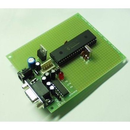
- 40 Pin PIC Development Board

40 Pin PIC Development Board
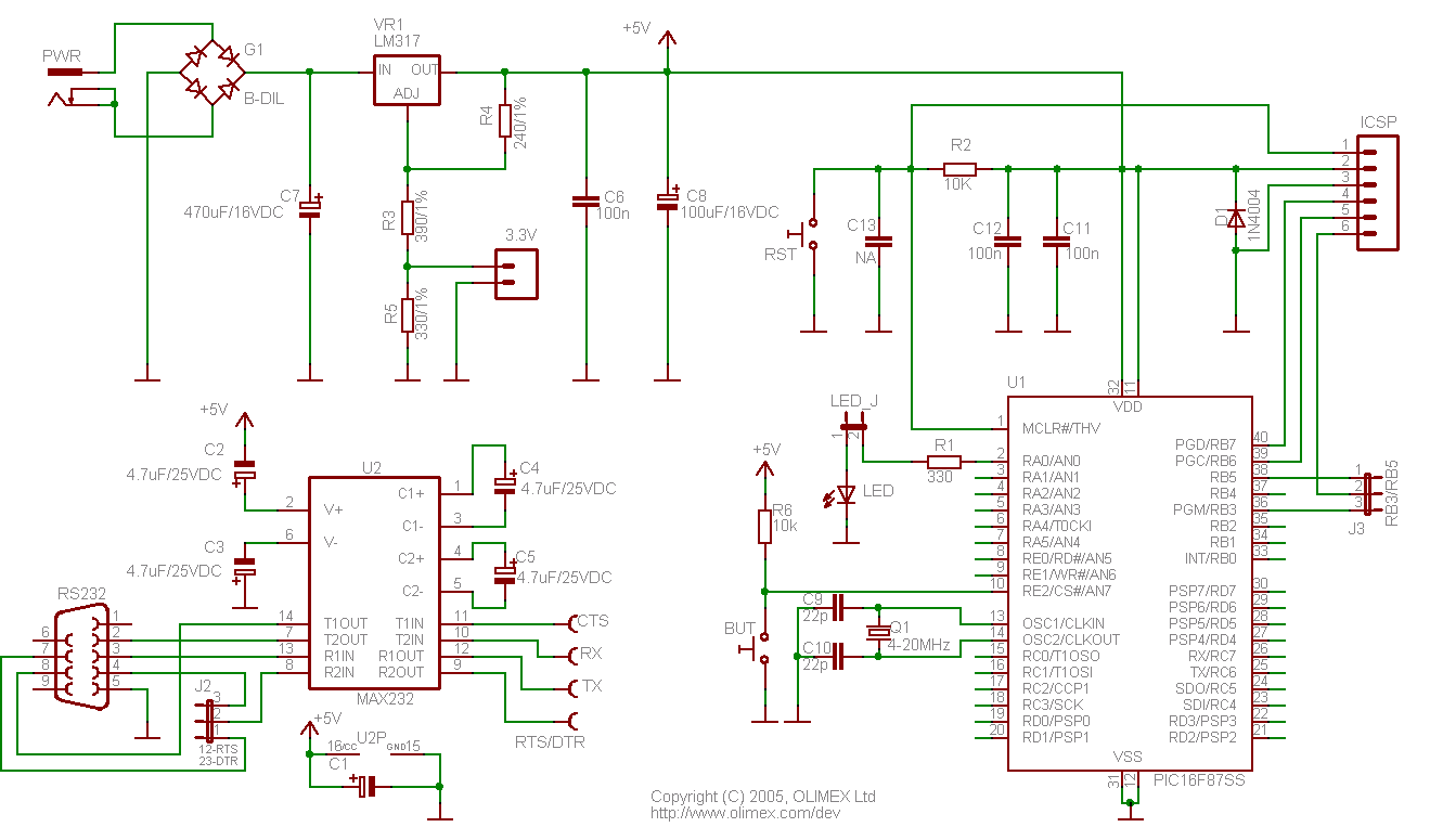
If you need lots of Analog to Digital channels, or plenty of program space (up to 32K!), this one is for you! Prototype board for 40 pin PIC microcontrollers with power supply circuit, 20MHz crystal oscillator circuit, RS232 port, ICSP/ICD programming port.
Note: Board does not come with PIC installed. Please see a list of related ICs below.
- FR-4, 1.5 mm (0.062"), green solder mask, white silkscreen component print
- Dimensions 100x80 mm (3,9x3,15")
- Four mounting holes
- Power plug-in jack
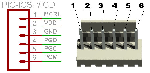
- ICSP/ICD connector for programming with PIC Programmers and Debuggers (for PICs with ICD support)
- Voltage regulator +5V, 78L05 and filtering capacitors
- LED to RA0 through jumper
- Quartz crystal oscillator circuit - 20Mhz
- DIL40 microcontroller socket
- RS232 DB9 female connector
- RS232 MAX232 interface circuit with Tx, Rx, CTS, DTR/RTS signals
- Extension slot on every uC pin
- Gird 100 mils
- Vcc, GND bus
40 Pin PIC Development Board Product Help and Resources
Core Skill: Programming
If a board needs code or communicates somehow, you're going to need to know how to program or interface with it. The programming skill is all about communication and code.
Skill Level: Competent - The toolchain for programming is a bit more complex and will examples may not be explicitly provided for you. You will be required to have a fundamental knowledge of programming and be required to provide your own code. You may need to modify existing libraries or code to work with your specific hardware. Sensor and hardware interfaces will be SPI or I2C.
See all skill levels
Core Skill: Electrical Prototyping
If it requires power, you need to know how much, what all the pins do, and how to hook it up. You may need to reference datasheets, schematics, and know the ins and outs of electronics.
Skill Level: Noob - You don't need to reference a datasheet, but you will need to know basic power requirements.
See all skill levels
Comments
Looking for answers to technical questions?
We welcome your comments and suggestions below. However, if you are looking for solutions to technical questions please see our Technical Assistance page.
Customer Reviews
No reviews yet.
I am very impressed with this item .... You can barely buy the components for this price. Having a board ready to go for this price. I'll be using this extensively. bought 3 spares
First off, I'd like to say this board is awesome. I will definitely buy more for my next projects. How can they build these so cheap??
However, I do have a few cons, which if fixed, would make this item over the top:
1. The one I got is not like the picture shows. Most of the installed parts near the edge of the board are shifted around. Don't plan on putting your own connector on the same side of the board as the power and serial port if you get a board like I did.
2. The holes in the side rows of the PCB are Vcc and GND. It is hard to catch this with the eye, so don't plan on using those holes for anything other than their intended purpose (it got me!), unless of course you want to drill a hole or cut etch.
3. TX and RX on the board white print are labeled wrong (in my opinion). Just remember that you need to hook up the white RX on the dev board to TX on the PIC, and the white TX on the dev board to RX on the PIC. Another user previously noted this.
4. The regulator is a LM317, which allows you to use on an on-board jumper to change from default 5V to 3.3V rail for Vcc (how cool is this??). The product description says 78L05 part, but it's not. Even the schematic shows this. Also, if you buy a Sparkfun Project Case for this, the regulator is soldered on the board and sits so high that you won't be able to close the lid. I bent mine (too much work to desolder/resolder for me) at an angle and barely got it to fit just right, just looks crummy now in clear case. :( Also, keep in mind the arrangement of parts on the board I got has the back of the regulator up against some electrolytic capacitors, so no room for a heat sink.
5. J3, as shown in schematic, is not a header jumper. There are 3 surface pads located under the PIC on the bottom of the board and you must solder alter this jumper to change it.
Sparkfun, looks like you need to overhaul this project description and update to the latest picture. The new arrangement of parts threw me for a quick redesign of my project, and luckily I had other options to handle not getting the board in the picture. A quick rewrite of the description and picture update would alert potential buyers to the above main cons I have.
Even with the above issues, this board is awesome and I will be buying again, and again.
I just thought I'd mention that the ICSP connector on this defaults to to connecting to RB3 for the PGM pin, but can easily be moved to RB5 for chips such as the PIC18F4431.
I love this board! I've used it for two different projects (Vdd=5V) and will buy another for my next project. Documentation is sparse, but following traces will help you figure it out. In addition to the note by Cpr. Crunch about voltage, note that the TX and RX labels should be connected to the RX and TX pins of your PIC's EUSART respectively. If you look at the RS-232 pinouts, MAX232 datasheet, and PIC datasheet, you'll see what I mean.