- Home
- Product Categories
- Development Tools
- Spartan 3E Breakout Board

Spartan 3E Breakout Board
Replacement: None. It's finally time for this board to step aside and make room in the catalog for more cool stuff. This page is for reference only.
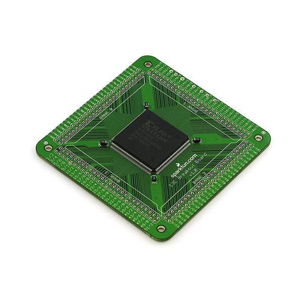
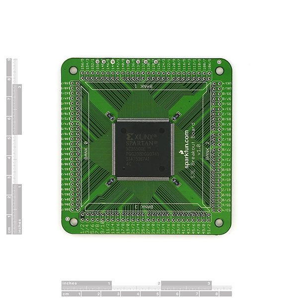
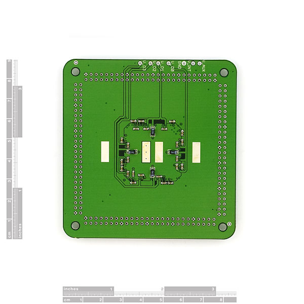
This is a simple breakout for the Spartan-3E FPGA from Xilinx. The 208-pin FPGA is brought out to 0.1" spaced, dual-row headers for every single pin. There are supporting decoupling and power capacitors for each bank of pins.
7 separate power pins are brought out to the edge of the board. Four pins are provided for the I/O voltage for each bank (for example: CMOS, TTL, RS232, etc for each bank). V_AUX and V_INT are also made available.
Comments
Looking for answers to technical questions?
We welcome your comments and suggestions below. However, if you are looking for solutions to technical questions please see our Technical Assistance page.
Customer Reviews
No reviews yet.
I would buy a few of these for my prototyping needs, too bad the price is legalized theft. I can design my own board, have them made by a professional PCB house and get the parts of the price of one of these. :-/
waaah. if you think there is enough market and their profits are so excessive, then you've clearly got a wonderful opportunity to go into business for yourself.
for anyone else: you're looking at $30 to buy just one of the chip, and probably $30 to get your hands on at least one board. can you layout the board, do the ordering, and assembly in less than an hour? if so, you're sufficiently skilled that your time is worth more than $10/hour.
What's the reasoning behind the oddly spaced power through-holes? It would be nice to be able to put 100mil headers on them...
100mil? Why would you want 4 inch headers? The board isn't even 4" wide!
100 mil = 0.1 inches * 26 = 2.6 inches.
The headers would have .1 inch spacing. Each header row would be about 2.6 inches long.
is this a 4-Layer? Or 2-Layer board? if its 2 layer then signal quality for sure not gona be good.
oh i didnt even look at it, its 2 layer.. but dont c a reason in it then. would be much better to have something like this with at least 4 layers.
Which set of Xilinx tools are you using? What have you downloaded?
Does anyone know what command to run to start Xilinx software in linux I run ubuntu? I would like to start my design before I buy the cables and FPGA.
if you did a standard install the actual program is located in the /opt/Xilinx directory from there (I think, I'm not in front of my computer at the minute) its ISE/Common/lin and then the program is called "ise" just double click on it.
Thanks so much for the example code. All the tutorials out there assume the diligent board which has the FPGA package type so the pin numbers are all incorrect when it comes to routing and mapping. It looks like the PQ package type just numbers the pins sequentially whereas the FPGA uses letters and numbers to identify the pins. The .ucf file in the sample cleared up any doubts I was having. Thanks Again!