
SMD How To - 6
Hot-air magic tricks!
Now for a magic trick. If you've got a leadless component (like a QFN CP2102), you can solder the component onto a tight pitch footprint without solder paste or expensive machinery (or a hot plate). This requires some soldering and a hotair rework station.

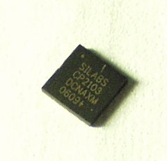
Here is a CP2103 that was pulled from the USB board shown earlier.


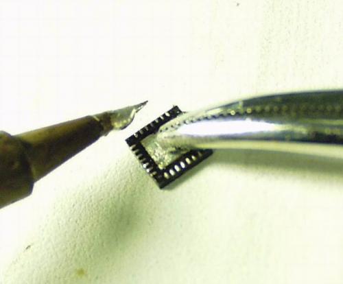
Here's what the bottom looks like. Notice the uneven pads and gunk in the middle.

I call this 're-balling'. Here I simply run a blob of fresh solder around all the pads evening them out and clearing any jumpers that may exist. The hemostats are there only to hold the IC down, otherwise it would stick to the end of the iron. Note that you want to avoid adding solder to the center pad.
If you do accidentally get a large blob of solder in the middle of the IC, you will want to clear it out with solder wick. Otherwise, if you try to hot-air solder the IC onto the PCB, the large blob in the middle of the IC will get squished out to the surrounding pads and cause bad jumpers.
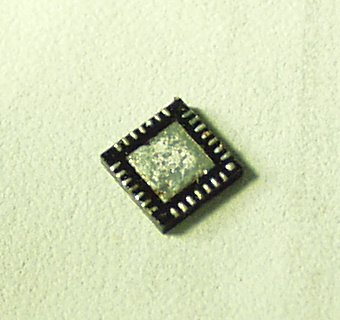

Here is the finished re-balling. It looks gunky, but it's actually pretty uniform. The balling helps add solder to pads so that when the IC meets the PCB with heat, there is something there to stick the two together. Normally you would solder the two together with an iron, but this is not possible with this footprint and leadless IC.
This balling and hot-air soldering technique can be used on BGA devices as well! Scary, but true.
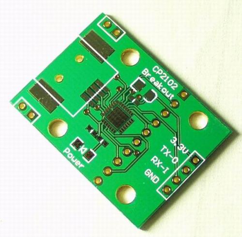

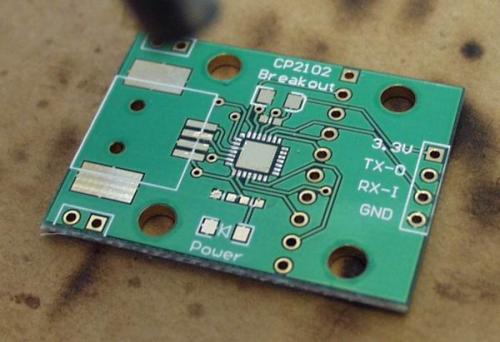
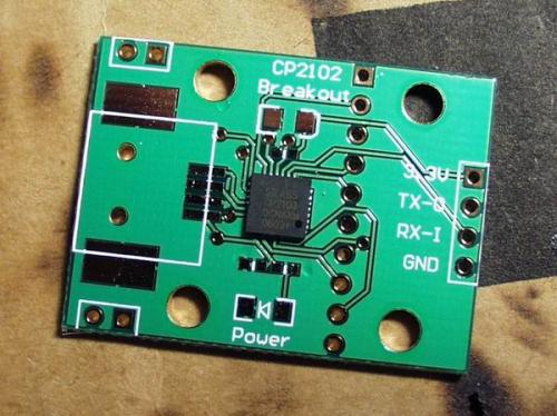
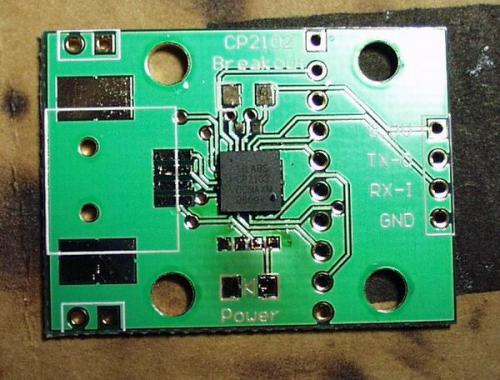
The new, clean board. Um, just ignore that this is a CP2102 board and we are throwing a CP2103 onto it...

Here you can see that I've added a similar balling to the PCB by swiping an iron with solder on the tip across all the pads. With a little work, you can even avoid jumpers between pads. This micron layer of solder will help when the two objects come together.
Note again - I have not added solder to the center pad. This is a common misconception and problem. Almost all center pads are ground connections in addition to ground connections on exterior pads (so you don't even need the center pad connection). Soldering of the center pad is very rarely required! Don't even worry about it. If you do add solder to the center pad, you will need to wick it away. This is a large center pad very close to the exterior pads (bad design on my part). The center pad will very actively suck solder towards it if you get sloppy. If you're designing your own footprint for a device, be sure to make the center pad smaller and away from exterior pads.
What's the big deal? What happens if you get solder onto the center pad? If the center pad becomes domed in a big way, and you hot-air the IC onto this domed pad, one of two things will happen. More than likely, you will press the IC down. The domed solder will squish to the exterior pads shorting many things to the center pad. Or if you don't press down, the IC will float a couple hundred microns above the PCB leaving all sorts of open connections. Bad news all around. A little solder is not a big deal but try to leave the center pad as flat as possible.
Various customers have recommended adding vias to the center pad so that you can 'feed' solder from the back side. This is a decent approach, but widely not needed. If you're soldering with an iron only, this is an ok idea - but I've only seen 2 ICs, in my lifetime so far, that required the center pad soldered to function. If you're prototyping, the center pad should be accounted for in your footprint, but don't lay awake at night worrying about soldering it. Finally, if you're using hot-air, more then likely there will be a minute amount of solder between the two pads, and even a mechanical connection may be enough of an electrical contact to take care of any center pad issue. In 6 words or less - don't worry about it.

Getting ready for some hot-air.

Here I've heated the PCB pads with hot-air for 5-10 seconds, placed the IC onto the pads and straight as possible, then held the IC in place while I remove the hot-air. The hot-air will BLOW away the IC if you don't hold it in place. Once the connections cool, take a look. More than likely, the IC is skewed like the image above - REALLY bad. All sorts of pads are where they shouldn't be, but don't despair! Hot-air is your friend!

Yea. That's really boo-bad initial placement.

Slowly bring the gun back over the IC. Rotate the gun in a circle slowly heating the PCB while not exposing the IC to too much air force. I heated this board/IC for 5-10 seconds. The IC righted itself and jumped into place! I did not touch the IC with tweezers or anything - only air. Really. I promise. Surface tension and hot-air are a fantastic thing. If the footprint is good, the IC will center and right itself using the solder at hand.
Now for the non-faint of heart - if you get really good, try 'bumping' the IC with your tweezers/hemostats in one hand and the gun aimed in the other (keeping things molten). If you bump lightly, the IC will literally slide slightly and then jump back into place once you remove your tool pressure. This is a good trick for trying to remove jumpers under the IC and pads without removing the IC completely.

So what happens if I sit with the gun aimed at one spot for 30 seconds? Here we see black nastiness around the Power LED. If exposed to excess heat over time, the PCB will delaminate, pop, smoke, hiss, smell horrible, and bubble up.

Bubble around the Power area.
Once the PCB delaminates, it's pretty much toast. Sometimes it'll work, other times traces will be broken from the stress. Don't worry about this - a little practice with the hot-air and you'll be repairing and salvaging ICs, PCBs, and parts with ease!
Page 7 - Video examples
I've only seen 2 ICs, in my lifetime so far, that required the center pad soldered to function
It's electrically the same as some other pins, yeah, but it's usually still important thermodynamically, since the big pad acts as a heatsink to dissipate heat into the ground plane. I've worked with amplifier chips that not only require this to be connected, but require a certain amount of continuous ground plane on the other side of the board, too.
Not connecting it or connecting it poorly might cause the device to fail prematurely. Running vias to the other side is probably a better idea.
Awesome tutorial! Will definitely be adding these techniques to my arsenal of knowledge.
To [Almost_there] : temperature of the soldered device should not exceed 260C (500F), in most cases (but check the device datasheet, some datasheets even have reflow profile charts, and you should try to follow those). I like to use a thermal probe connected to a multimeter, right next to the device and monitor the actual temperature. I set the temperature on hot air station to about 300C-350C. You need to control the temperature by how far you keep the nozzle from the device. Start 5-6 inches away then slowly move towards the device, with spiral motion , if you see you're exceeding 500F move back up or you could damage the device. If you don't have hot air station a regular hot air gun will do (if it can reach 260C/500F).
Also, this walk-through might be of interest to anyone attempting to do leadless smd soldering for the first time:
http://starlino.com/surface_mount_reflow.html
Wow! This is such a great tutorial! I wish I would have known this a week ago... I wouldn't of fried a pcb while trying to salvage it.
I would also like to ask at what temperature and at what pressure should I set the hot air gun (approximately at least)?
Hi all,
Thanks for this great tutorial.
However, I have a question regarding this tutorial. You might have mentioned this in a previous tutorial, so accept my apologies if you have.
I see that all the boards in the tutorials are 'professionally' made.
What would happen if I tried to solder a DFN/QFN chip on an 'amateur' made PCB?
I have access to the below equipment:
JetStar Premium -Inkjet Film for artwork production
(I have tested the above film which will go down to 250um or less)
Vacuum UV Units
PA310 Tri-Tank Unit (Develop, Wash and Etch)
(I should point out this is not an advert for the company producing the above equipment, but an honest question).
I would be planning to solder the chip using a Hot Plate, but I do have access to a hot air gun as well.
I would rather keep the PCB production in house. This is the reason I am asking this question.
Regards
Alex
Why not his from mouser for small quantity silver solder paste?
557-7459
7459
Wahl Soldering Irons/Accessories SILVER SOLDER PASTE Page 2,081 In Stock
Click
to
View
1: $5.03
12: $4.29
Hello,
It is not recommended to add solder to the DFN package pads, as this will potentially delaminate or break the bond wires. I found this out the hard way. If you want to add solder, add it to the PCB lands, then use solder wick to pick up the excess. Inspect with ~10X magnification, to verify that each land has roughly the same amount of solder. The best method I found is the solder swipe method, but the soldmask (SM) should be exposed enough to get the iron tip to touch the PCB copper trace and not interfere or touch the DFN package. I found if I scraped away the SM on the traces, I could tin those copper trace, then using liquid solder flux, the solder would wick along the copper trace and then to the DFN pad. Solder paste is a pain, unless you are using a stencil, since it is very difficult to dispense the right amount and at the same time be centered on the PCB land. Use lead based solder, forget the non-lead stuff, as it does not wick very well and requires more heat.
Refer to : TI "SLUA271A–June 2002–Revised September 2007" TI "SCBA017D"
Cheers Rick
This and other tutorials seem to be missing several pictures. Could someone double check those to make sure they are coming up correctly? Thanks!