Beginner's Guide to KiCad
 Nate
Nate 
Editing a PCB Layout
Before we start editing the PCB, here are the keyboard shortcuts in KiCad's Pcbnew that we will be using frequently in this tutorial:
- + - Press to switch next layer.
- - - Press to switch to previous layer.
- m - Move item.
- b - Update ground polygon pours.
- Delete - Remove a trace or component.
- x - Route new track.
- v - Add through via.
- n - Next grid size. Use with caution. There will be tears if you use a grid outside of 50mils or 25 mils.
- Page Up - Return to the top copper layer.
- Esc - Escape mode or whatever command in progress and return to normal pointer mode.
- ctrl+z - Undo. Use liberally to undo any mistakes.
- ctrl+s - To save. Make sure to save often!
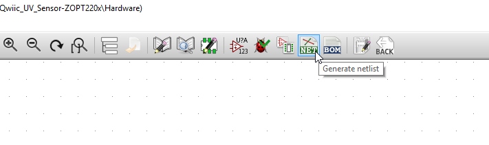
Generate Netlist
We've got our schematic, now let's get the new 4.7uF cap placed on the board. From the schematic, click on the 'Generate netlist' button.
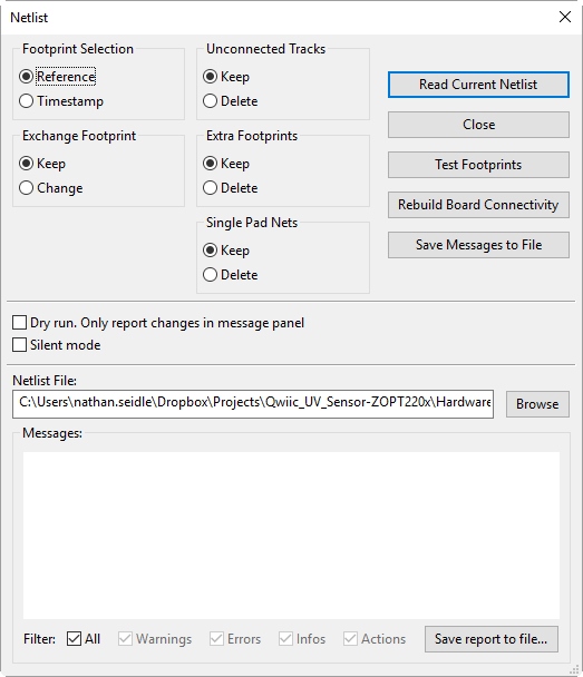
You'll see the following window:
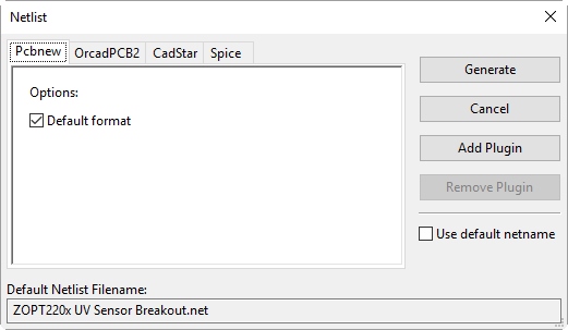
KiCad is powerful. And with this power, comes an overwhelming number of options. Lucky for us, we are just scratching the surface so we don't need to fiddle with any of these options. Simply press enter or click 'Generate' to confirm this screen. KiCad will ask you where you want to save the netlist as a ** *.net** file with the default location being the project folder. Again, press enter or click 'Save' to confirm.
Configuring Layer Colors
Return to the main project window and double click the ** *.kicad_pcb** file.
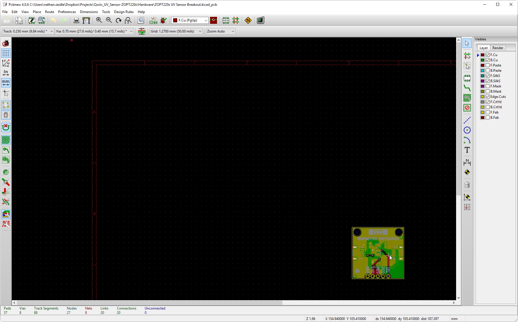
Welcome to PCB editing. Of all the differences between EAGLE and KiCad it was the look within PCB layout that threw me off the most. Under the View menu you will find three other views: Default, OpenGL, and Cairo. I prefer OpenGL. Lets switch Canvas to OpenGL for now.
Your mouse wheel does what you expect: Zoom In/Out and Pan by Clicking.
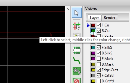
I don't like the layer colors! Ya, me either. To change the layer colors, on the right side menu use your mouse wheel to click on the green square next to B.Cu (bottom copper layer). I prefer the following layer colors:
- Red 2 (Default) for F.Cu (Top Copper)
- Blue 4 for B.Cu (Bottom Copper)
- White for F.SilkS (Front Silk Screen)
- Yellow 3 for B.SilkS (Bottom Silk Screen)
- Gray 3 for Edge.Cuts (a.k.a board outline or dimensional layer in EAGLE)
- Gray 2 (Default) for F.CrtYd (Denotes the total board space required on the top layer for the component)
Pressing '+' and '-' will switch between top and bottom copper layers. This is useful when you need to view a certain layer.
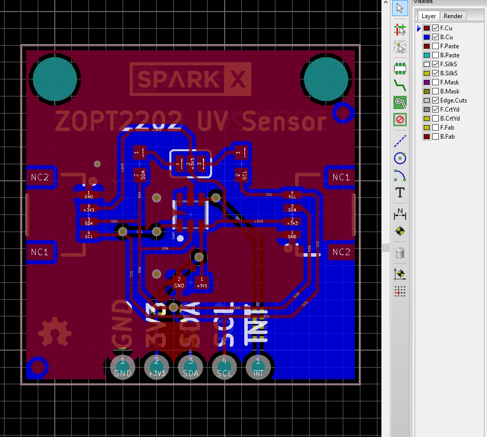
It's all cosmetic but these layer colors make it easier for me to see what's going on.
Be sure to poke around the Render tab (next to the Layer tab), namely the Values and References check boxes.
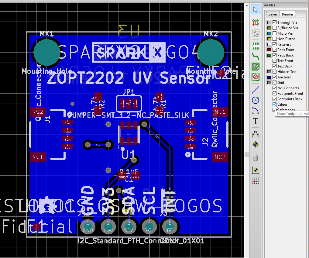
I find the Values and References extremely distracting when turned on so I leave them OFF. Many designers live and die by these values, so use as needed.
Adding a Footprint
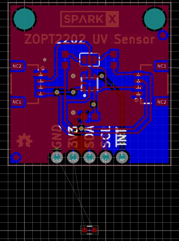
Aren't we here to add a 4.7uF cap to the board? Where is it? It's nowhere, sorry.
What's going on? We failed to assign a footprint to the capacitor we added in the schematic. Remember, KiCad does not link schematic components to footprints the same way EAGLE does. We have to specifically connect a footprint to each schematic component that was added.
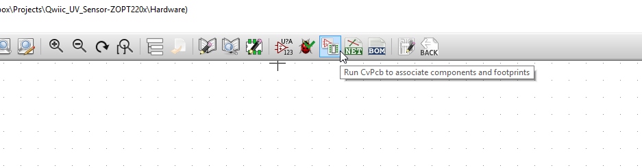
Navigate to back to schematic and click on the 'Run CvPcb' button to associate components and footprints:
If this is the first time you've run CvPcb you'll get this warning:
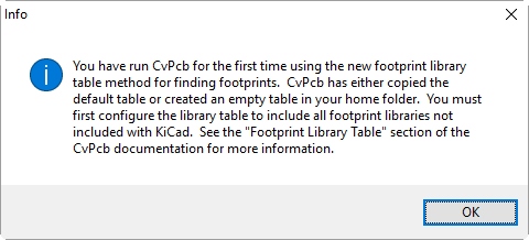
Simply click through it.
Depending on how many libraries you have installed, this may take up to 30 seconds. We will make this better later in the tutorial but for now, be patient.
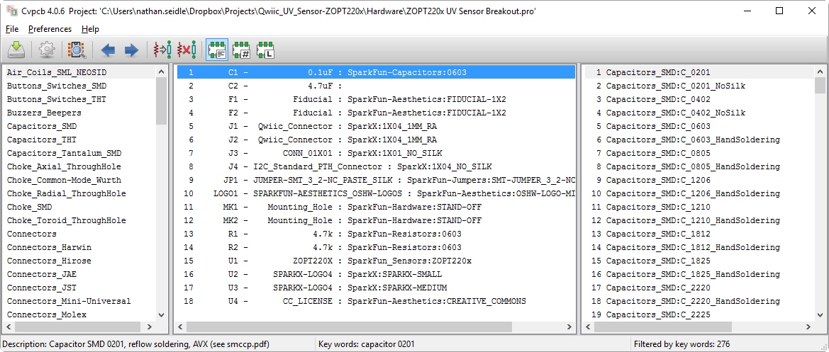
In the left column is all the footprint libraries that KiCad ships with. In the middle is the list of components in your schematic. On the right is any footprint that may work with the highlighted component in the middle. Your job is to double click on the footprint on the right that goes with the component in the middle.
To make life easier click on the 'View selected footprint' button.
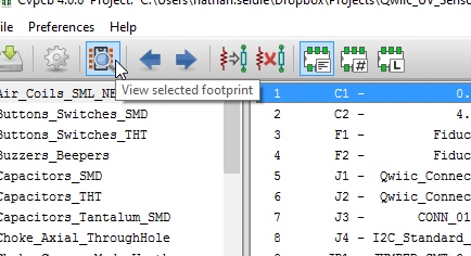
Now you can preview the footprint as you click down the list in the right.
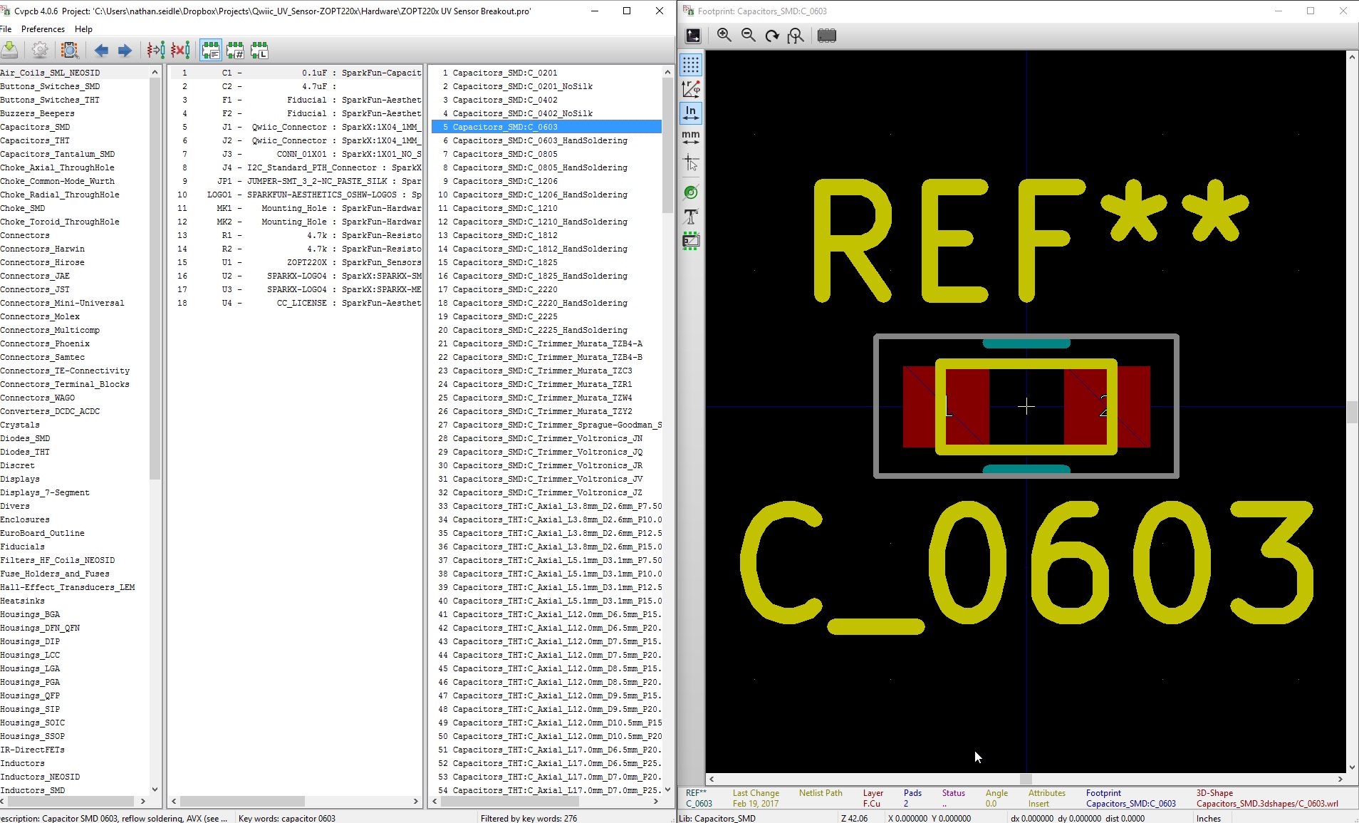
In Windows, I press and hold the Windows button and press the left arrow and release. This will lock the CvPcb window on one side. Then select and lock the Footprint Preview Window to the right. This allows us to flip through footprints in the left window while seeing the preview on the right.
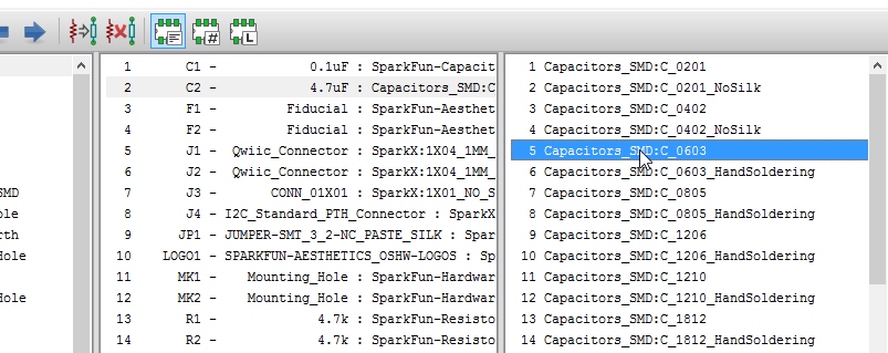
Highlight C2 in the middle column. Then double click the Capacitors_SMD:C_0603 in the right column. C2 should now be assigned a footprint.
Re-Generate Netlist
Close the CvPcb window and click 'Save and Exit'. We need to re-export the Netlist. Remember how to do that? Click the 'Generate netlist' button again, press enter twice. Open to the PCB editor either from the schematic or from the project window.
Hey! It's still missing! We changed things, so we need to import the netlist! Remember how? Click on the 'Read netlist' button and you should see this window:
Click 'Read Current Netlist' and 'YES' to confirm. You can also hit enter twice. You should see the new capacitor near the board.
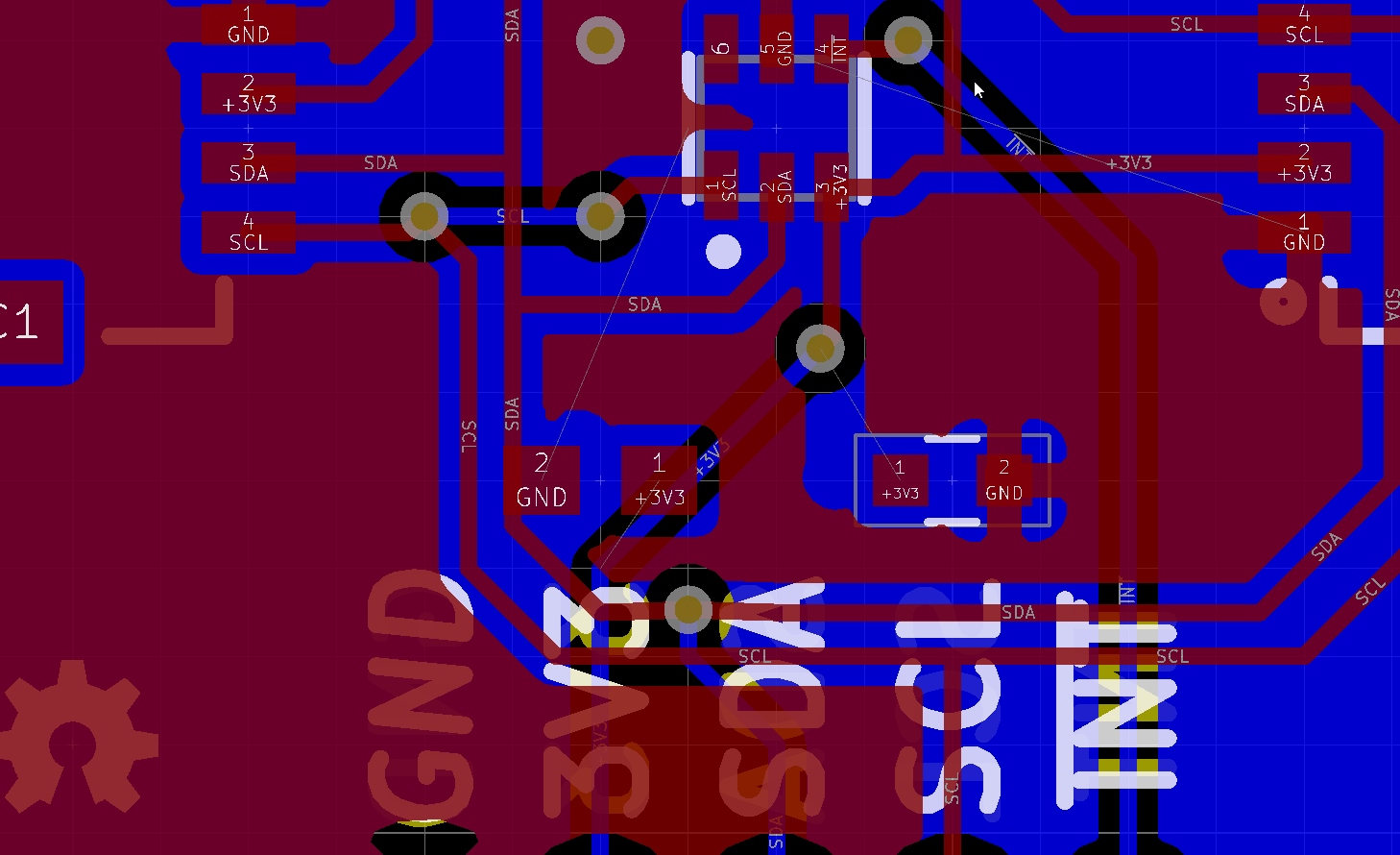
This is a decoupling cap so let's put it next to the 0.1uF cap that is already there. Start by hovering over the new cap and press 'm' for move.
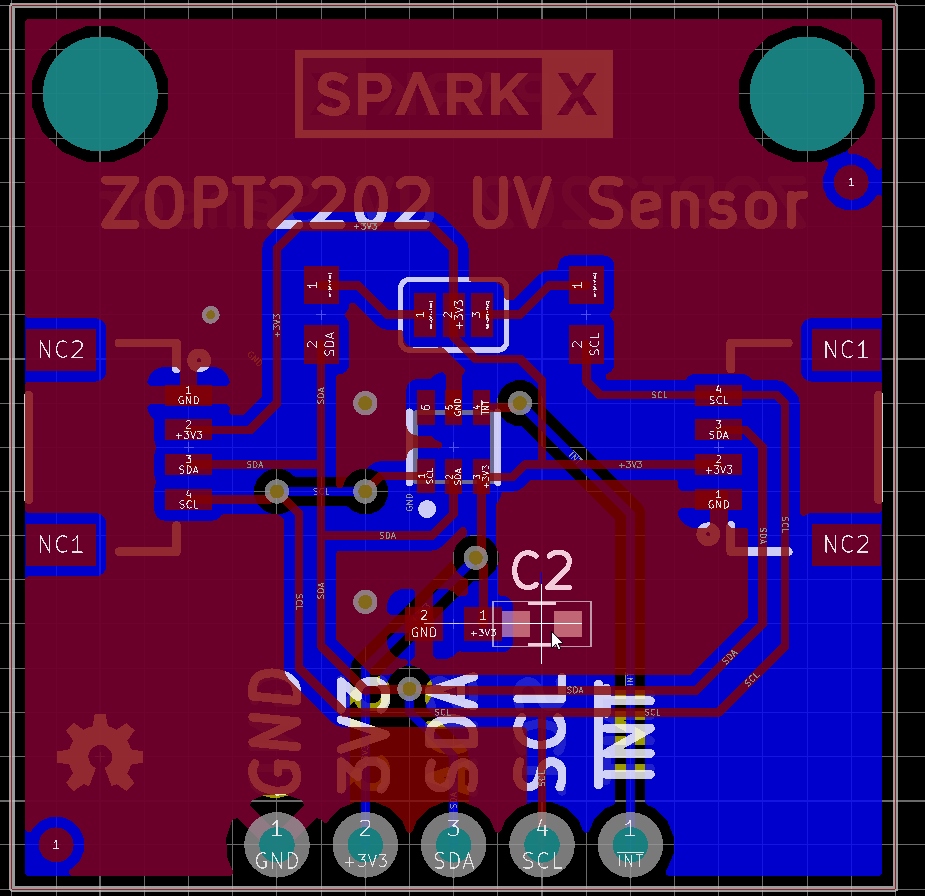
Left click to place the capacitor. Now press 'm' over the 0.1uF cap in the way by moving it to the left.
Press 'b' to update the GND polygon pours.

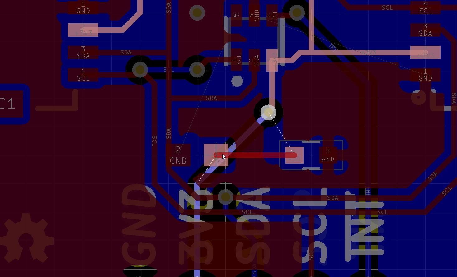
We've got some traces to fix but this isn't too bad. Hover over the bits of traces that you want to remove and press 'Delete'. Let's delete the trace and via that is under the capacitor's +3v3 terminal. If your pointer is over multiple items (as shown in the image below with the cursor over both the trace and capacitor), KiCad will pop up a menu to clarify your selection. This is basically asking you to pick which one you want to operate on.

If you ever run into a problem press 'Esc' to return to default pointer mode. If you ever delete something wrong press 'ctrl+z'.
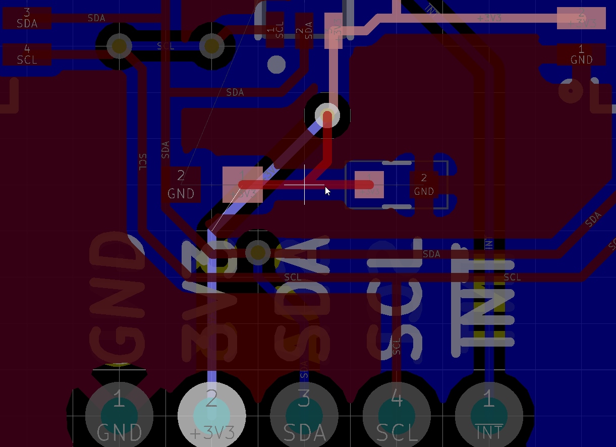
Once you've removed most of the offending traces, you can begin routing by pressing 'x'.
Single click on the pad that has the gray air-wire and drag it to the pad that it needs to connect to. Single click again to lock the wire in place. Press 'b' to update the polygons.
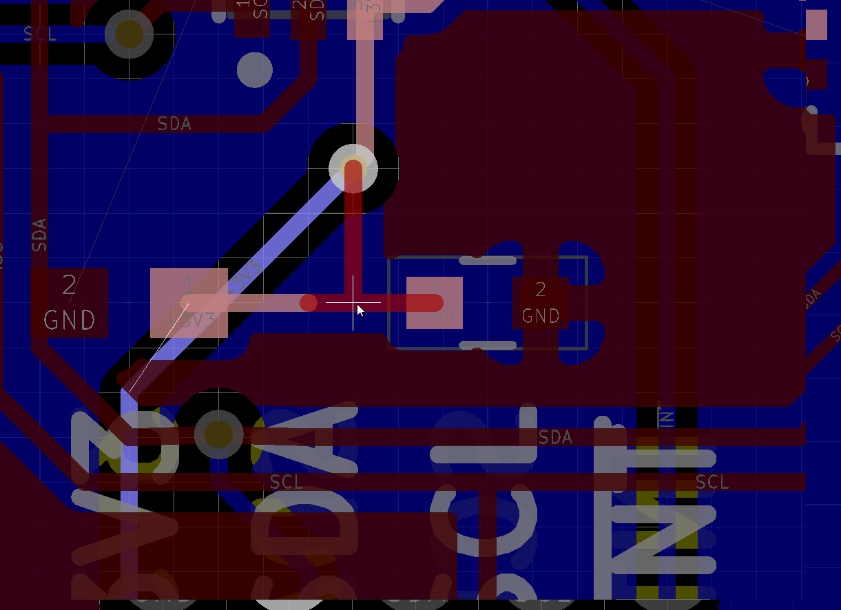
In the image below, KiCad is trying to route this trace in an odd way. If we place the trace here it will create an acute angle which is generally bad (read up on "acid traps"). We want the trace to be a T intersection. We need to change the grid.
Press 'n' to go to the next grid size. I needed to hit 'n' only once to go to the 0.25mil grid to get this nice intersection, you may need to get to a finer grid. You can also find this in the menu options under "Grid: 0.0635mm (2.5mils)."
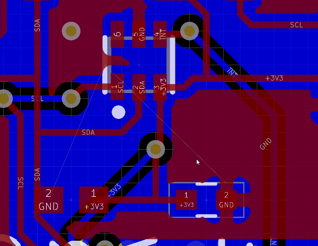
In the image below, I am routing the GND air wires. This is not really needed because the polygon pour connects the two pads but it does illustrate how good the 'magnetic' routing assistance is in KiCad. It's very quick and easy to go from pad to pad.
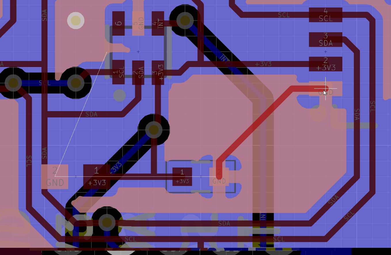
We have two air-wires left. To get these we'll need to place vias down to the bottom layer. Start by pressing 'x' and clicking on the start of the capacitor's air wire for GND again.
Bring the trace out.
When you've reached open ground press 'v' to create a via. Single click to place the via and KiCad will automatically start routing on the bottom layer. Press 'Esc' to stop laying down traces; the polygon pour will take it from here. Pressing 'Page Up' will take you back to the top layer.

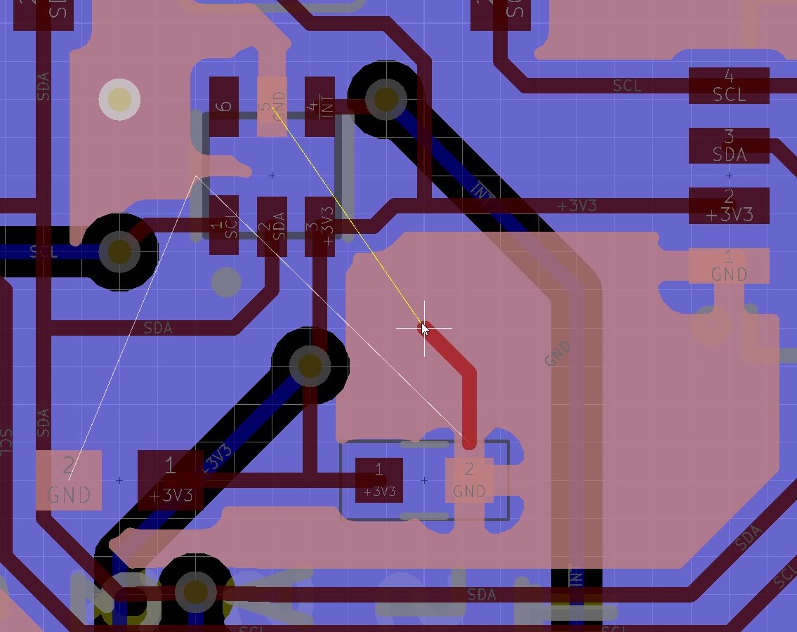
To get this last air wire, you can try clicking on the GND pad of the 0.1uF cap but annoyingly KiCad won't start routing?! Why?! It's actually a good thing: the SDA trace is too close (overlapping actually) to the GND pad on the 0.1uF cap. By not letting you start routing KiCad is saying that trying to put a trace here would violate the DRC rules. What to do? Rip up the SCL and SDA lines to make some room.
Aha! Much better. Press 'x', click on the capacitor's GND terminal, bring the trace out, and press 'v' to drop a via in this area. Hit escape to stop routing (let the polygon take care of it). Finally, press 'Page Up' to return to the top layer view.
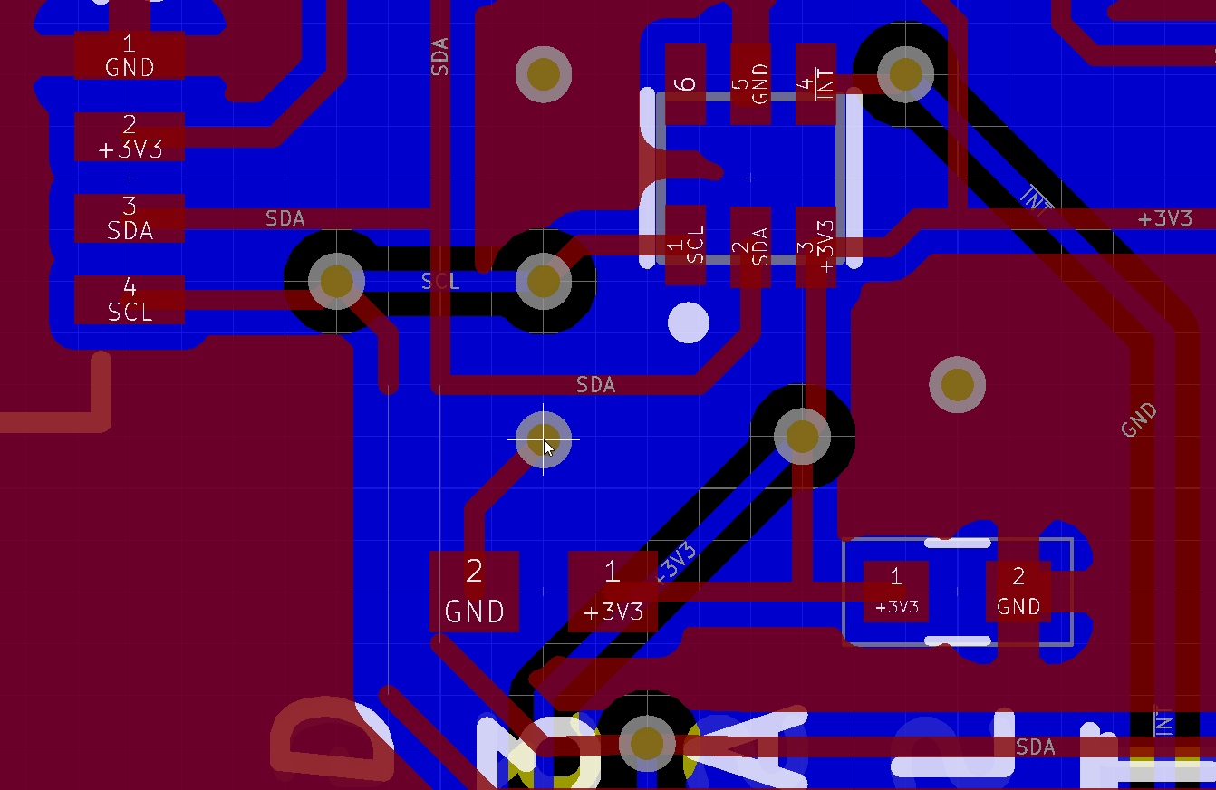
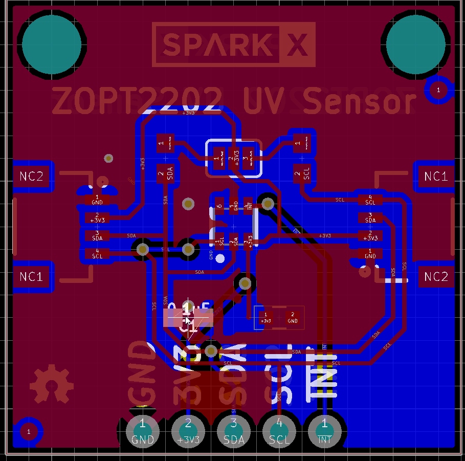
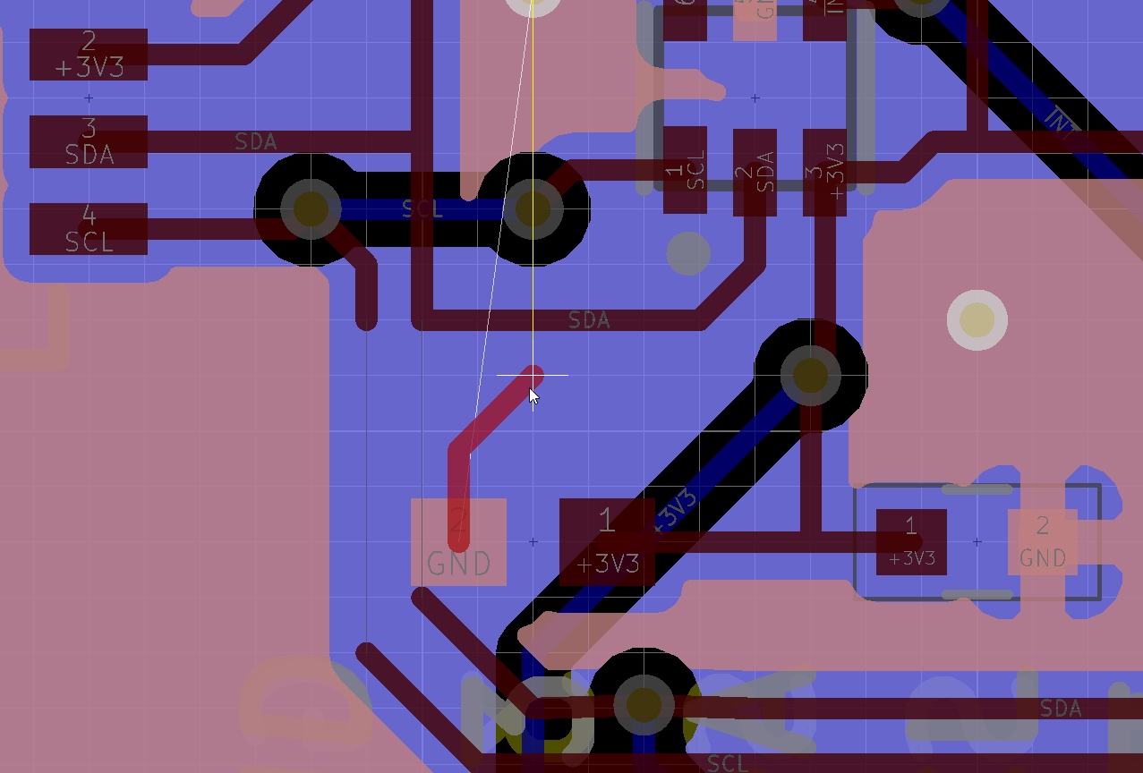
Use the 'Delete' and 'x' buttons to re-route the SDA and SCL lines to finish up this board. Then press 'b' to update the polygons. The board should look similar to the image below.
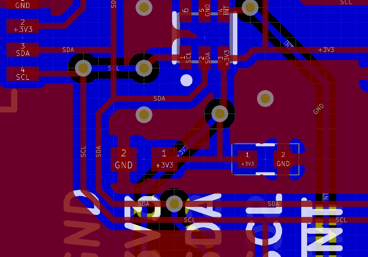
Congrats! We have finished routing the footprints. Now let's run the DRC to see if we're legal.
How to Remove a Component's Footprint from a PCB Layout
Before we continue let's go over the process for modifying or removing a component from a PCB layout. For example, let's say that you wanted to remove an extra capacitor or resistor from a design. You would do all the regular steps:
- Delete device from the schematic.
- Export the netlist by clicking the generate netlist button.
- Import the netlist into PCB Layout by clicking on the read netlist button.
The difference is a few import settings:
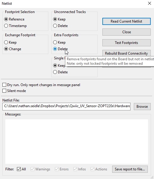
During the netlist import the default settings are to 'Keep' exchange footprint and to 'Keep' extra footprints.
Here, we need to change two things:
- Exchange Footprint -> Change: This will allow footprints to change
- Extra Footprints -> Delete: This will remove any extra footprints that remain
You may also want to 'Delete' unconnected tracks to clean up any left over tracks from the component you removed.