Constant Innovation in Quality Control
 QCPete
Pad Size, Fillets, and AOI
As part of our constant quest to improve our testing thoroughness, in the spring of 2011 we purchased our first AOI machine (automated optical inspection). After watching it run a few panels of boards, we quickly named it "Disco Stu". If you've ever seen an AOI machine run, than you probably remember a lot of flashing lights of various colors. It's actually quite a spectacle to watch and usually has a pretty good "Ahhhhhh" effect on tours.
The AOI's primary purpose is to look at boards and tell us if there are any manufacturing errors. It checks for 3 things:
Marks (to tell us if the part is in fact on the board and the polarity is correct)
Solders (to tell us if there is sufficient amounts of solder and how well it reflowed)
Lead banks and Toes (to tell us if any legs on an IC jumpered together and/or do not have sufficient solder on the toe of the leg)
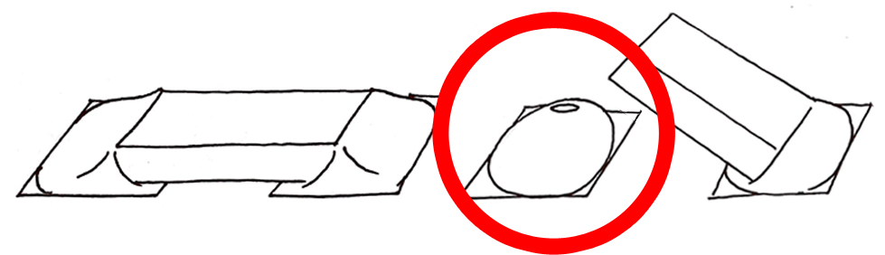
As we programed more recipes (unique to each of our 500+ in house assemblies) we started to notice that the machine was having difficulty inspecting some of our components - particularly our 0603 solder joints. The reason was that the solder joint was forming underneath the component legs. This made it difficult for the top down camera to see. Also, the solder was not forming a fillet on it's edge. In stead, it was basically forming a little bubble below.
There was a trend in our earlier designs to use 0402 sized packages on the PCBs and then populate an 0603 sized part. This was done in an effort to save space, while still using a component size that is moderately easy to handle with a set of tweezers.
We did this for years, and it didn't seem to be that big of a problem. But now, with our new AOI machine, we wanted to fine tune our processes even more and narrow in on any manufacturing errors -- no matter how small they may have been. We wanted to start catching the very rare cases where an 0.1uF capacitor would tomebstone and sneak through production to your workbench.
To understand how this problem was effecting the AOI, we need to look closer at how the machine does it's testing. It actually looks at the same component in a variety of ways under three different colors:
White (all white LEDs pointing straight down on the board)
Red (this is primarily useful to see flat surfaces, because the red light is reflected to the side if the surface is anything but flat)
Red, Green and Blue (which are actually hitting the board from 3 unique angles)
The following graphic is combination of four different images. Each image was taken of the same row of components under a unique lighting. This particular design has 0402 pad sizes with 0603 parts populated.
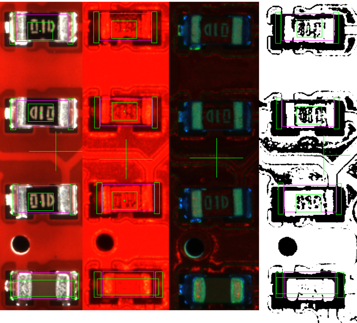
On the right side, we are also seeing the binary bitmap image that the AOI can generate to help inspect for good solder reflow. The binary bitmap is created from the image taken under red light. The white pixels represent flat spots on the board, and the black pixels represent curved surfaces. In this way, a bare pad (without any solder on it) would reflect the red light and would show up as all white pixels. The software can count the white pixels of a designated area on the board and determine if there is sufficient solder present.
If you look at either side of the components, you can see that there is very little pad space to analyze. Most of it is covered up by the component and the solder. This makes it difficult for the AOI to test for sufficient solder.
The next image is a similar row of components, but this time they have the correct 0603 sized pads with 0603 parts populated.
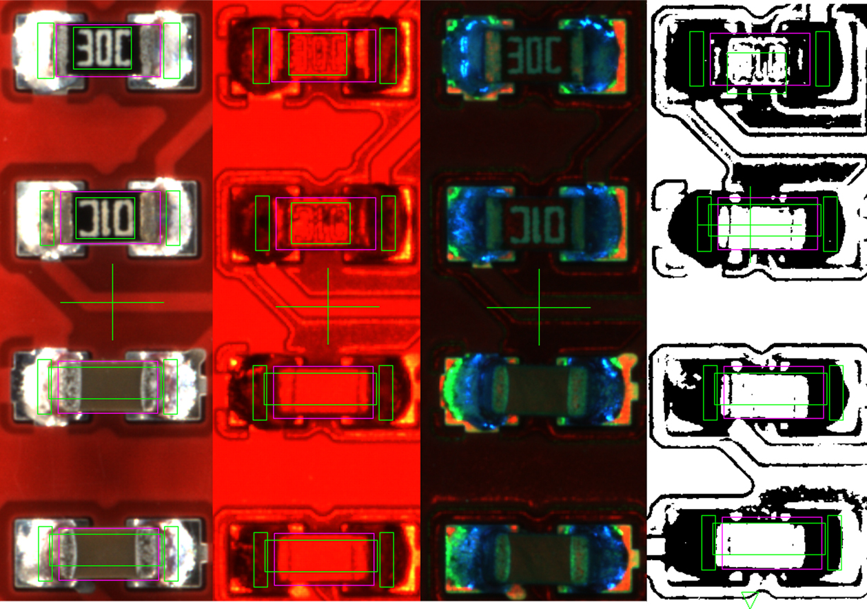
Notice how there is more pad visible from this top down view. We can now compare the amount of white and black pixels and verify that there is sufficient solder.
This also helps us determine whether or not the part has slightly tombstoned. When you get a tombstone, the solder left on the pad will usually pillow and have a nice shiny flat spot on the top. The AOI can look for this flat spot under red light and see if the part did not reflow properly.
We have recently made a big push to revise a lot of our older designs to include true 0603 footprints. Each member of our QC team has made an effort to revise at least one design a month (sometimes two!).
Also, all future designs will have the correct pad size. In fact, the production QC team has become very involved whenever designing a new footprint for a new part. We want to ensure that the pad size and shape will promote the best possible solder reflow and that we can utilize our AOI to catch any possible errors.
In an effort to create the best footprint possible, we have recently developed a new technique using images of the bottom side of a component in Eagle. If you like, you can read more about that at our tutorial, Making Custom Footprints in Eagle.