Designing PCBs: Advanced SMD
 Nate
Nate 
Creating Vias
Now let’s talk vias. Vias are a hole in the PCB that have metal running down the inside of the hole so that the traces on the front of the board are electrically connected 'via' the hole to the back of the board.
Press F9 to go into routing mode and look for the Drill box in upper right corner. The default via size in Eagle is 0.02362205” (or more sanely 0.6mm). I change this to 0.02” (or 0.5mm if you please) and press enter to make Eagle save that size.
There is nothing magical about 0.02". This is a size that we've found most PCB fab houses can drill without too many tolerance issues. It’s also small enough to ‘tent’ over with soldermask making the board look a little better.
Press F9 to route from a pad. While you’re routing hold the shift key while you left click. This will drop a via and you’ll continue to route on the top layer. Now click the middle mouse wheel. This will drop you to the bottom layer and you can keep routing.
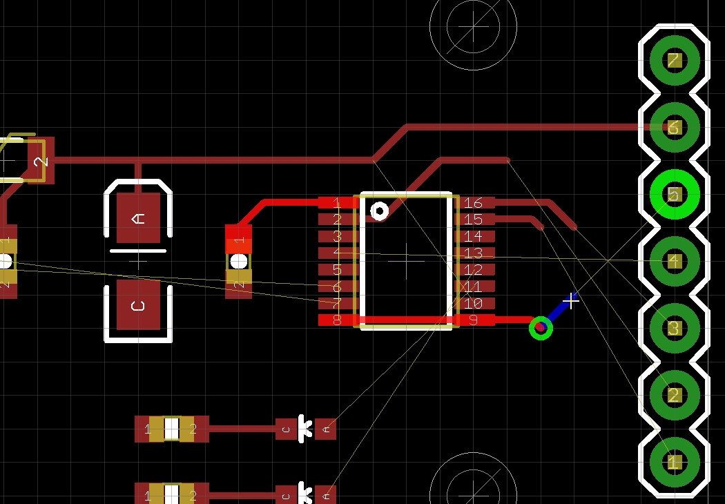
Continue to route some of the other nets.
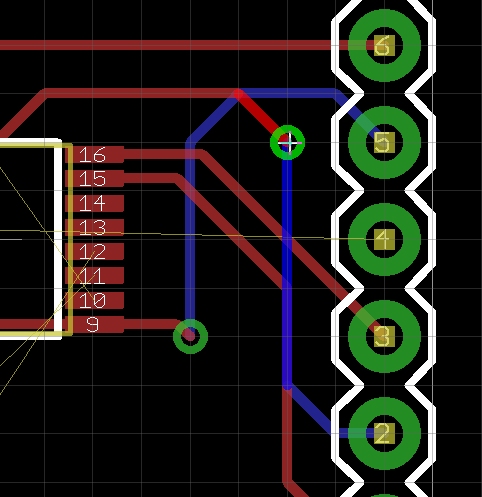
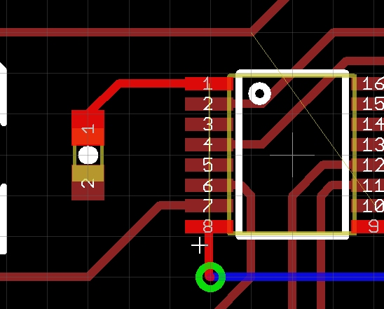
The above routing will work, but if we bump the highlighted via downward, we can straight out the blue trace a bit. Like this:
Nitpicking? Absolutely. But bumping various routes around can make the overall routing a lot cleaner over time.
Note that I keep nearly everything onto the 0.05” grid. This keeps routing and spacing a lot easier. The size (0.05”) is reasonably trivial. The important piece is that all the components and general routing are kept on the same grid.
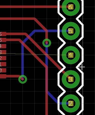
We’ve got two problems here. Two wires could be routed without vias if we ripped up the 8 to 9 route. The two wires also cross over themselves. Re-arranging the LEDs will fix this.
Fixed. However you may note the trace connecting Pin 11 on the FT230 is off grid. While routing, hold the Alt key to jump 'off grid'. Going off grid is perfectly fine but as a rule of thumb, I try to keep on the grid as much as possible.
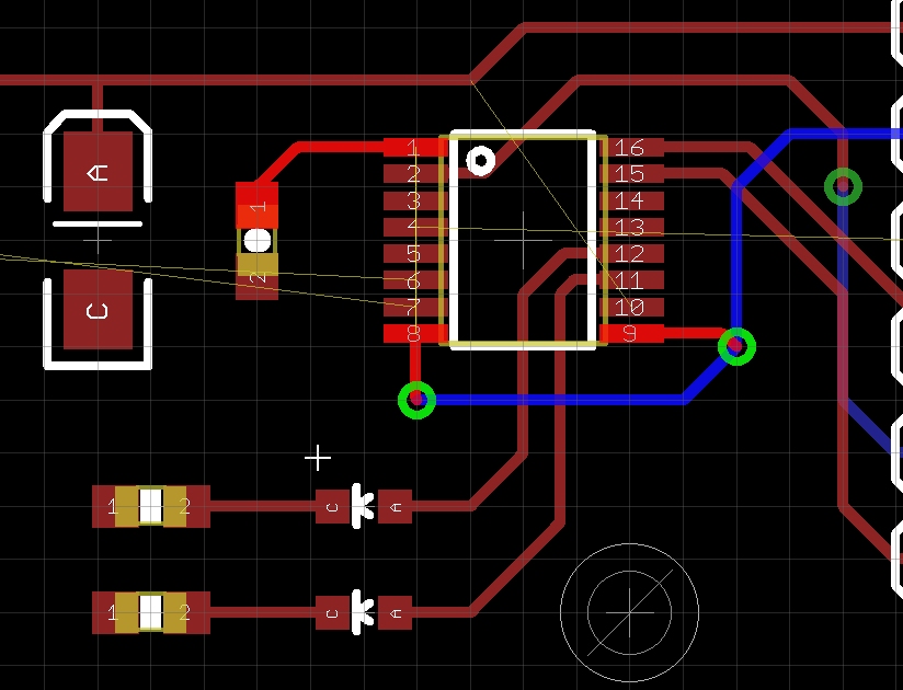
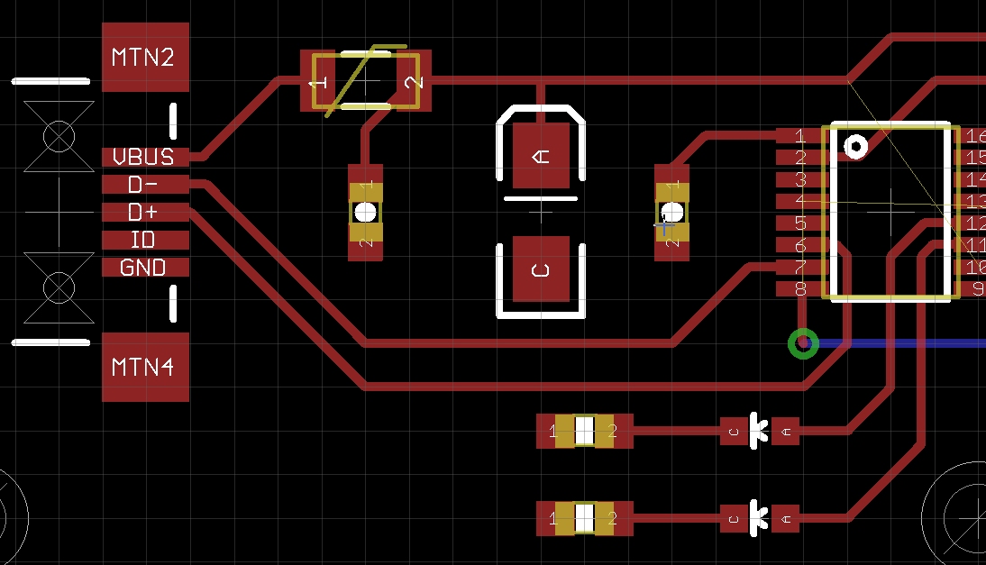
Removing the 8 to 9 route also opened it up so that we could route the D+ and D- traces directly to the IC.
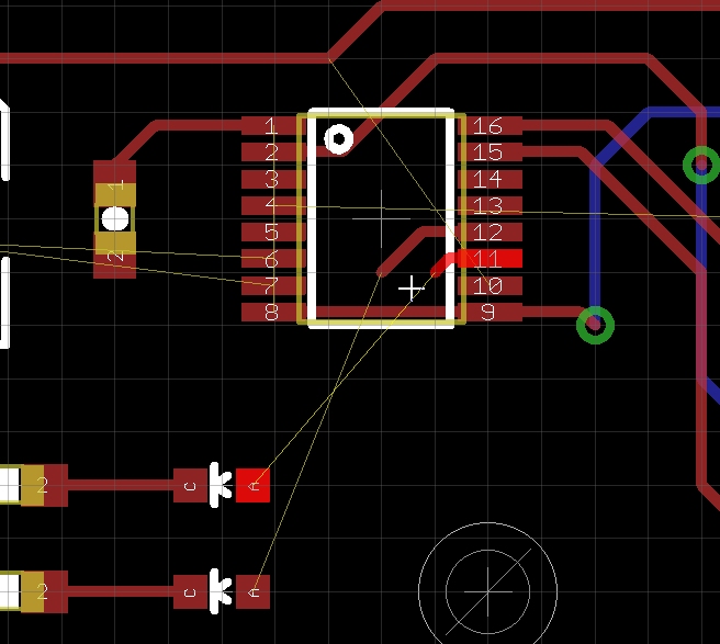
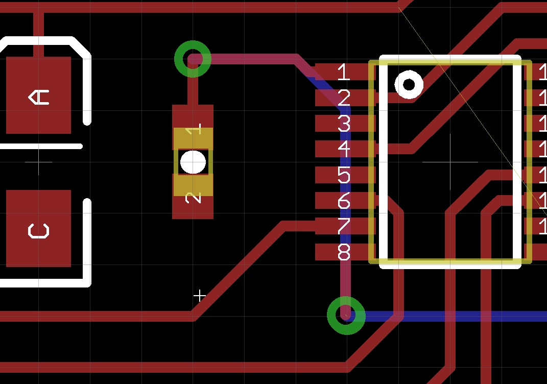
Ah! Neat. If we move some stuff around, we can get !CTS routed without needing a via.
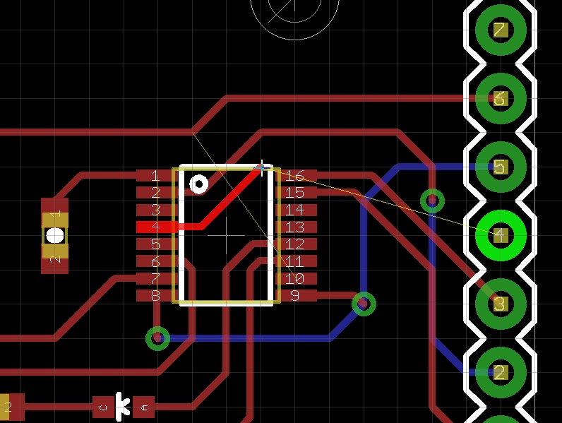
There’s obviously a DRC error here but we can fix it when need be. Let’s just leave it in case other things change.
Now I need to get pin 8 connected to pin 1, but Eagle won’t let me start routing from the lower via - it keeps wanting me to route from pin 8. To get around this, I am going to rip up some of the traces near the via so that I can have a starting point. Press Alt+F9 then click on a trace to rip it up.
I ripped up a small trace which gave me an airwire that I started routing from.
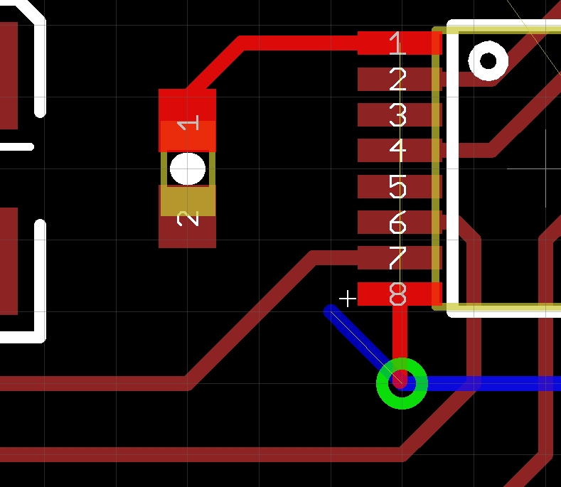
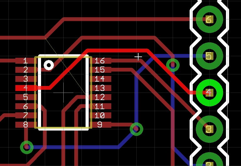
Re-routed. Note I still have a very small airwire that I need to route. Not hard, press F9, click on the airwire, click again, and it’ll route.
Next up - we create polygons!