How to Sell Your Widget on SparkFun
 jimblom,
  Pearce
Designing for (SparkFun) Manufacture
The schematic and PCB designs are the heart of most SparkFun products. Over the last 10+ years, we've designed hundreds of unique PCBs, and produced millions of widgets, so we know what adjustments to the design will make our production process flow as smoothly as possible.
Those adjustments have found their way into a loose set of rules that we know to follow, but you might not. Designing your product with these rules in mind will give you a head start, and it'll also make your product pitch more attractive to us. The less work we have to put into scrubbing your design, the faster we can start building and shipping it!
- Design your PCB in EAGLE -- The collaborative process is easiest if we're both speaking the same EDA language. There are dozens of design tools out there, but we've gotten really accustomed to EAGLE. If you're not familiar with the software, consider checking out some of our tutorials for help getting started.
- Use our EAGLE libraries -- By using our set of EAGLE footprints and parts, you're better assured that the parts in your design will also be on our inventory shelves. You'll also be using the footprints that our quality-assurance team has painstakingly crafted to help optimize AOI and other testing.
- Unless your part is a kit, aim to use as many surface-mount (SMD) parts as possible. Our production team is most efficient, when they're letting the pick-and-place/reflow oven combo do most of the busy work.
- For common passives (resistors, capacitors, etc.), try to us 0603 parts or bigger (0805, 1206, ...).
- If a part has multiple footprints, and you're unsure of which one to use, consider checking the Eagle files of one of our live boards and comparing against that.
PCB Design Specifications
In as many designs as possible, we try to keep our board layouts within this set of specifications:
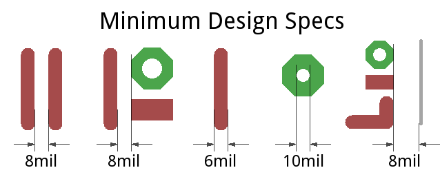
- Minimum Trace Width: 0.006" (6 mil)
- Minimum Trace Clearance: 0.008" (8 mil)
- Trace-To-Board Edge Clearance: 0.008" (8 mil)
- Minimum via Drill Diameter: 0.01" (10 mil)
- Default Board Width: 1.6mm
EAGLE Design Rules
Further to those minimum specifications, here are some more EAGLE-specific design rules:
- Board Frame
- Create the board frame on a 0.1" grid. Make the lower left corner start at (0, 0).
- Change the line width of the board frame to 0.008"
- Board frame will be square unless called for by special requirements of the design.
- Grid
- All parts are placed on a 0.005" grid. If possible, use a .05" grid.
- Make sure all 0.1" headers are lined up on a 0.1" grid. Keep it breadboard compatible!
- Packages
- Use 0603 packages for resistors and capacitors.
- Traces
- Use 10 mil (0.010") traces in general.
- 8 mil traces can be used when necessary, 6 mil is absolute minimum.
- Use thicker traces (as thick as possible) on power and charging traces.
- Keep at least 8 mil of space between traces.
- Route with straight lines and 45 degree corners only. No right angles in trace routing, but T-intersections are okay.
- Route from pads. Avoid routing into the pads- this causes traces to be not centered on a pad. Traces should enter and exit center of pad at 90 degree angle.
- Pours
- Use ground pours on the top and bottom layers.
- Change the "Isolate" setting on ground pours to 12 mil (0.012").
- Vias
- If something is soldered into a hole (header, connector, prototype vias, etc), use a via with a larger annular ring so that it is easier to solder. For normal prototyping vias, use 0.04" hole with a 0.074" diameter.
- Set the default via size to 0.020."
- 0.010" is the smallest allowed via size. Only change from the default if absolutely necessary.
- Via size is defined by the "Drill" parameter in the DRC.
- Misc
- Add a version code on the bottom copper layer, and revise the version code on every revision!
- Use the standardized I2C layout: GND, VCC, SDA, SCL.
- The autorouter can only be used on prototypes. Hand routing and touch-up of the autorouter is expected for production boards.
Make sure to load the Sparkfun.dru for the DRC check. Pull the most up-to-date version of the Sparkfun.dru from GitHub. Don't use the default settings!
PCB Aesthetics (Labeling)
When the bare PCB is your product, it doesn't hurt to dress it up and make the board look nice and polished. Here are some EAGLE-specific design rules that we follow to make our boards look as good as possible.
- Labels
- Label the name of the board appropriately.
- Label any LED with its purpose (power, status, D4, Lock, etc).
- Label all connectors (Vin, Port1, Batt, 5-9V, etc).
- Label pins where applicable (Tx, Rx, Power, +, Charger, etc).
- Label switches and switch states (On/Off, USB, etc).
- Label any extra information (ie. axes on gyros, accelerometers, etc).
- Makes sure labels are on a straight line- add a line in the tDocu layer to make sure the labels line up.
- Text should be 0.032" minimum and 15% ratio, vector font.
- Logos
- Every board should have the full SparkFun logo or at least the smaller SFE Flame. Add the
LOGO-SFEpart to the schematic. Make sure to put this part in the lower right hand corner of the schematic. - Every board should have the Open Source Hardware Logo unless otherwise specified. Look for
OSHW-LOGOin the library and add it to the schematic. This should go in the lower right hand corner as well.
- Every board should have the full SparkFun logo or at least the smaller SFE Flame. Add the
- Misc
- Components that are grouped together in the PCB layout will be grouped together in the schematic. Draw boxes to show functional groups.