MicroMod nRF52840 Processor Hookup Guide
 El Duderino, MAKIN-STUFF
Hardware Overview
In this section we'll cover the nRF52840 SoC in more detail as well as other components included on the MicroMod nRF52840 Processor.
M.2 Connector
All of our MicroMod Processors come equipped with the M.2 MicroMod Connector, which leverages the M.2 standard and specification to allow you to install your MicroMod Processor board on your choice of Carrier Board.
 |
 |
| M2 Connector from the Front | M2 Connector from the Back |
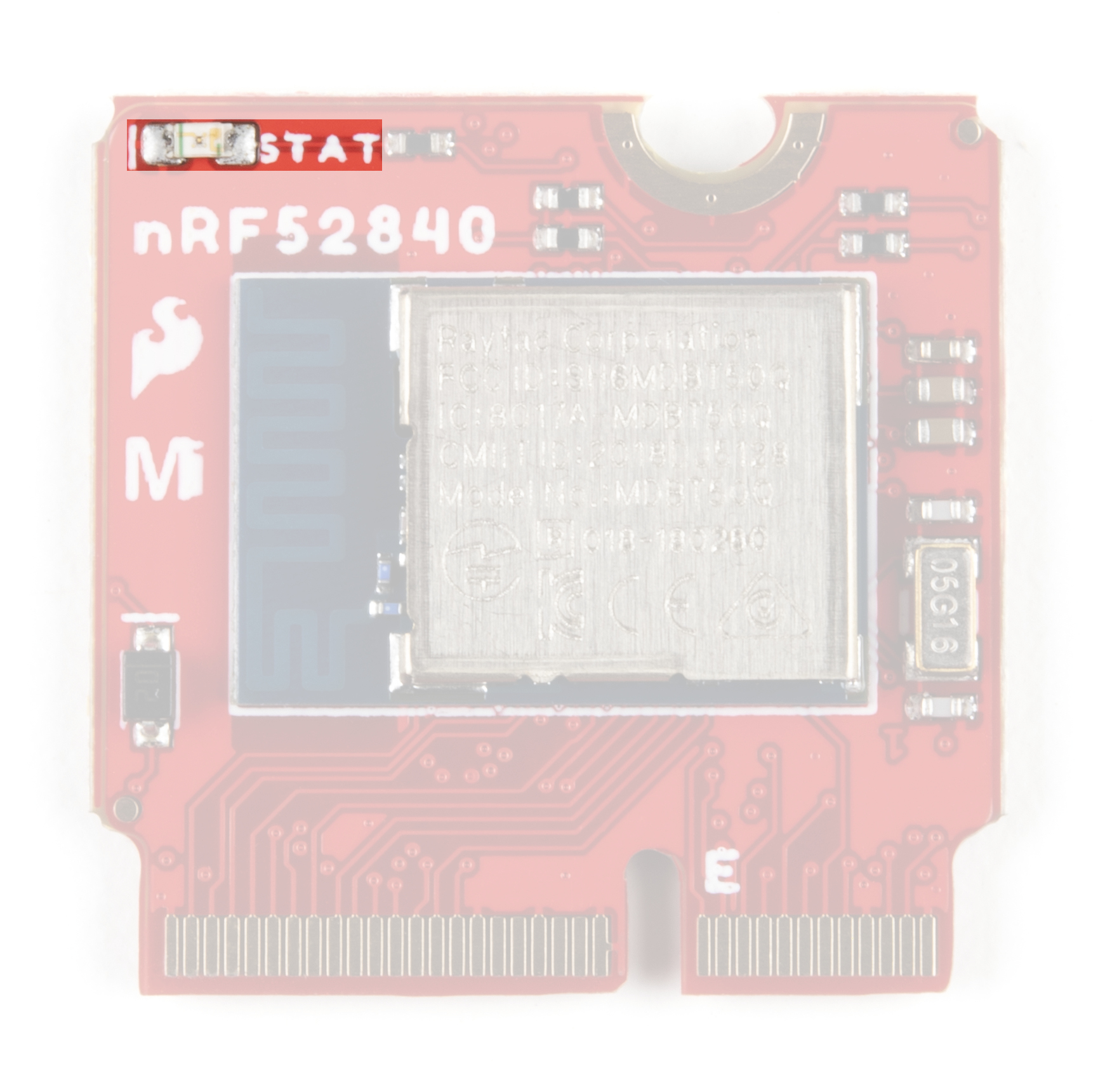
nRF52840 MDBT50Q Module
This Processor features the nRF52840 SoC from Nordic Semiconductor. The specific module is from Raytac which includes a built-in PCB antenna. Refer to the MDBT50Q Module Datasheet and nRF52840 IC Datasheet for full specifications on the IC and module.

The nRF52840 combines an ARM Cortex-M4 CPU and 2.4 GHz Bluetooth transceiver to provide a versatile and powerful microcontroller with Bluetooth 5.0 wireless capability. The transceiver also works with Bluetooth mesh, IEEE 802.15.4(Thread & Zigbee), ANT and Nordic's proprietary 2.5 GHz RF protocol to communicate with other Nordic devices.
The nRF52840 Processor board uses the Arduino Nano 33 BLE Bootloader as opposed to the USB Bootloader found on the SparkFun Pro nRF52840 Mini.
Flash IC
Along with the nRF52840 module, the Processor also includes external flash memory in the form of the 128Mb (16M x 8) W25Q128JV SpiFlash IC from Winbond Electronics. The flash IC is connected via SPI on the nRF52840. For full details on the Flash IC, refer to the datasheet.

The flash IC uses the secondary SPI bus (SPI1) and its Chip Select pin is tied to a dedicated pad on the nRF module (P0.12). Writing to the flash IC requires some extra work involving adjusting the SPI definitions in the variant file and is not recommended for anyone but advanced users. Writing to the Flash IC is beyond the scope of this tutorial.
STAT LED
The STAT LED is tied to a dedicated pin on the nRF module (P0.13) and can be used as a status LED or as a built-in LED. Control it directly in Arduino by writing to LED_BUILTIN.
nRF52840 Processor Pin Functions
The nRF52840 has a ton of awesome features including (but not limited to):
- ARM Cortex-M4 CPU with floating point unit (FPU), 64MHz
- 1MB internal Flash -- For all of your program, SoftDevice, and file-storage needs!
- 256kB internal RAM -- For your stack and heap storage.
- Integrated 2.4GHz radio with support for:
- Bluetooth Low Energy (BLE) -- With peripheral and/or central BLE device support
- Bluetooth 5 -- Mesh Bluetooth!
- Nordic's proprietary RF protocol -- If you want to communicate securely with other Nordic devices.
- Interface Options
- USB -- Turn your nRF52840 into a USB mass-storage device, use a CDC (USB serial) interface, and more.
- UART -- Serial interfaces with support for hardware flow-control if desired.
- I2C -- SparkFun's favorite 2-wire bi-directional bus interface
- SPI -- If you prefer the 3+-wire serial interface
- Analog-to-digital converters (ADC) -- Six pins on the nRF52840 Processor support analog inputs though four are used for other functionality on the MicroMod Processor.
- PWM -- Two dedicated Pulse-Width Modulation interface pins.
- PDM -- Pulse Density Modulation interface. The PDM module generates the PDM clock and supports single and dual channel data input.
- GPIO -- Eleven dedicated General Purpose I/O pins.
Users who wish to alter pin functionality can modify the default board definition or use their own custom one but these can result in issues interacting with SparkFun Carrier Boards. If you decide to create or use a custom nRF52840 Processor board definition with a SparkFun Carrier Board, take note of the pins used for components (sensors, displays, etc.) to maintain compatibility. The board variant files can be found in the nRF52840 Processor Hardware GitHub Repository.
I2C
As you may have guessed from our extensive Qwiic System, we love communicating with devices using I2C! The nRF52840 Processor features two I2C buses. The main I2C bus has dedicated pins connected to MiroMod pads 12/14, along with a dedicated Interrupt pin connected to MicroMod pad 16. The primary I2C Bus will almost always be connected to a Qwiic connector on your Carrier Board.
If you want a second I2C bus, the nRF52840 has SDA1 and SCL1 on MicroMod pads 51 and 53. To use this second bus, initialize it by calling Wire1.begin();.
UART
The nRF52840 Processor has three UARTs available. The primary UART is tied to USB_D± (MicroMod pads 3 and 5) for serial communication over USB. This is used for your standard serial upload as well as serial prints in Arduino. The secondary UART is a hardware UART tied to MicroMod pads 19 (RX1) and 17 (TX1). The tertiary UART is another hardware UART tied to MicroMod pads 20 (RX2) and 22 (TX2).
In Arduino, use the following calls to send data over the three UARTs:
Serial- Communication over USBSerial1- Communication over RX1/TX1Serial2- Communication over RX2/TX2
SPI
The nRF52840 Processor features two SPI buses; SPI & SPI1. The primary SPI bus is tied to MicroMod pads listed below:
- CIPO (Controller In/Peripheral Out) - MicroMod pad 61
- COPI (Controller Out/Peripheral In) - MicroMod pad 59
- SCK (Serial Clock) - MicroMod pad 57
- CS (Chip Select) - MicroMod pad 55
SPI1 is tied to the flash IC and the pins are broken out to the M.2 connector on the MicroMod pads listed below:
- CIPO1/SDIO_DATA0 - MicroMod pad 64
- COPI1/SDIO_CMD - MicroMod pad 62
- SCK1/SDIO_CLK - MicroMod pad 60
- CS1/SDIO_DATA3 - MicroMod pad 70
- SDIO_DATA1 - MicroMod pad 66
- SDIO_DATA2 - MicroMod pad 68
Audio
The nRF52840 supports audio input processing through Pulse-Density Modulation (PDM). The pins used are:
- PDM_DATA - P0.26 , MicroMod pad 52. This is the PDM data signal.
- PDM_CLOCK - P0.25, MicroMod pad 50. This is the PDM clock signal.
For more information on how to process audio signals using PDM on the nRF52840 Processor, refer to section 6.15 of the nRF52480 Datasheet as well as this example for the MicroMod Machine Learning Carrier Board.
Dedicated Pins/GPIO
Finally, along with all the interface options, the nRF52840 Processor has two pins dedicated for each of the following functionalities: Analog Read/Input, Digital I/O and Pulse Width Modulation. The nRF52840 Processor also has eleven general purpose I/O pins.
Dedicated Pins
- A0 - ADC0/P0.04 , MicroMod pad 34 (Input Only!)
- A1 - ADC1/P0.05 , MicroMod pad pad 38 (Input Only!)
- D0 - P0.27 , MicroMod pad pad 10
- D1 - P1.08 , MicroMod pad pad 18
- PWM0 - P0.06 , MicroMod pad pad 32
- PWM1 - P0.16 , MicroMod pad pad 47
General Purpose I/O pins
- G0 - GPIO0/P0.29 , MicroMod pad 40
- G1 - GPIO1/P0.03 , MicroMod pad 42
- G2 - GPIO2/P1.13 , MicroMod pad 44
- G3 - GPIO3/P1.12 , MicroMod pad 46
- G4 - GPIO4/P1.11 , MicroMod pad 48
- G5 - GPIO5/P0.17 , MicroMod pad 73
- G6 - GPIO6/P1.06 , MicroMod pad 71
- G7 - GPIO7/P1.04 , MicroMod pad 69
- G8 - GPIO8/P1.14 , MicroMod pad 67
- G9 - GPIO9/P0.09 , MicroMod pad 65 - Shared with NFC1
- G10 - GPIO10/P0.10 , MicroMod pad 63 - Shared with NFC2
MicroMod Pinout
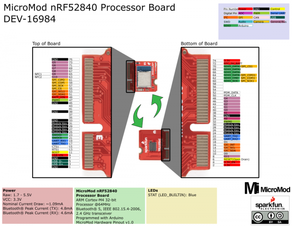
Users looking for a complete pin map can find it the table below or you can refer to the schematic.
| AUDIO | UART | GPIO/BUS | I2C | SDIO | SPI0 | Dedicated |
| nRF52840 Arduino Pin |
Alternative Function |
Primary Function |
Bottom Pin |
Top Pin |
Primary Function |
Alternative Function |
nRF52840 Arduino Pin |
|---|---|---|---|---|---|---|---|
| (Not Connected) | 75 | GND | |||||
| 3.3V | 74 | 73 | G5 | 17 | |||
| RTC_3V_BATT | 72 | 71 | G6 | 38 | |||
| 32 | SDIO_DATA3 | SPI_CS1 | 70 | 69 | G7 | 36 | |
| 23 | SDIO_DATA2 | 68 | 67 | G8 | 46 | ||
| 22 | SDIO_DATA1 | 66 | 65 | G9 | NFC1 | 9 | |
| 21 | SDIO_DATA0 | SPI_CIPO1 | 64 | 63 | G10 | NFC2 | 10 |
| 14 | SDIO_CMD | SPI_COPI1 | 62 | 61 | SPI_CIPO | 2 | |
| 19 | SDIO_SCK | SPI_SCK1 | 60 | 59 | SPI_COPI | 31 | |
| - | 58 | 57 | SPI_SCK | 28 | |||
| - | 56 | 55 | SPI_CS | 20 | |||
| - | 54 | 53 | I2C_SCL1 | 24 | |||
| 26 | PDM_DATA | 52 | 51 | I2C_SDA1 | 33 | ||
| 25 | PDM_CLK | 50 | 49 | BATT_VIN / 3 (0 to 3.3V) | 30 | ||
| 43 | G4 | 48 | 47 | PWM1 | 16 | ||
| 44 | G3 | 46 | 45 | GND | |||
| 45 | G2 | 44 | 43 | - | |||
| 3 | G1 | 42 | 41 | - | |||
| 29 | G0 | 40 | 39 | GND | |||
| A1 | A1 | 38 | 37 | - | |||
| GND | 36 | 35 | - | ||||
| A0 | A0 | 34 | 33 | GND | |||
| 6 | PWM0 | 32 | 31 | Module Key | |||
| Module Key | 30 | 29 | Module Key | ||||
| Module Key | 28 | 27 | Module Key | ||||
| Module Key | 26 | 25 | Module Key | ||||
| Module Key | 24 | 23 | SWDIO | ||||
| 39 | UART_TX2 | 22 | 21 | SWDCK | |||
| 37 | UART_RX2 | 20 | 19 | UART_RX1 | 42 | ||
| 40 | D1 | 18 | 17 | UART_TX1 | 35 | ||
| 15 | I2C_INT | 16 | 15 | UART_CTS1 | 41 | ||
| 11 | I2C_SCL | 14 | 13 | UART_RTS1 | 34 | ||
| 8 | I2C_SDA | 12 | 11 | BOOT (Open Drain) | |||
| 27 | D0 | 10 | 9 | USB_VIN | |||
| - | 8 | 7 | GND | ||||
| RESET# (Open Drain) | 6 | 5 | USB_D- | ||||
| 3.3V_EN | 4 | 3 | USB_D+ | ||||
| 3.3V | 2 | 1 | GND |
| Function | Bottom Pin |
Top Pin |
Function | ||||||
|---|---|---|---|---|---|---|---|---|---|
| (Not Connected) | 75 | GND | |||||||
| 3.3V | 74 | 73 | G5 / BUS5 | ||||||
| RTC_3V_BATT | 72 | 71 | G6 / BUS6 | ||||||
| SPI_CS1# | SDIO_DATA3 (I/O) | 70 | 69 | G7 / BUS7 | |||||
| SDIO_DATA2 (I/O) | 68 | 67 | G8 | ||||||
| SDIO_DATA1 (I/O) | 66 | 65 | G9 | ADC_D- | CAM_HSYNC | ||||
| SPI_CIPO1 | SDIO_DATA0 (I/O) | 64 | 63 | G10 | ADC_D+ | CAM_VSYNC | |||
| SPI COPI1 | SDIO_CMD (I/O) | 62 | 61 | SPI_CIPO (I) | |||||
| SPI SCK1 | SDIO_SCK (O) | 60 | 59 | SPI_COPI (O) | LED_DAT | ||||
| AUD_MCLK (O) | 58 | 57 | SPI_SCK (O) | LED_CLK | |||||
| CAM_MCLK | PCM_OUT | I2S_OUT | AUD_OUT | 56 | 55 | SPI_CS# | |||
| CAM_PCLK | PCM_IN | I2S_IN | AUD_IN | 54 | 53 | I2C_SCL1 (I/O) | |||
| PDM_DATA | PCM_SYNC | I2S_WS | AUD_LRCLK | 52 | 51 | I2C_SDA1 (I/O) | |||
| PDM_CLK | PCM_CLK | I2S_SCK | AUD_BCLK | 50 | 49 | BATT_VIN / 3 (I - ADC) (0 to 3.3V) | |||
| G4 / BUS4 | 48 | 47 | PWM1 | ||||||
| G3 / BUS3 | 46 | 45 | GND | ||||||
| G2 / BUS2 | 44 | 43 | CAN_TX | ||||||
| G1 / BUS1 | 42 | 41 | CAN_RX | ||||||
| G0 / BUS0 | 40 | 39 | GND | ||||||
| A1 | 38 | 37 | USBHOST_D- | ||||||
| GND | 36 | 35 | USBHOST_D+ | ||||||
| A0 | 34 | 33 | GND | ||||||
| PWM0 | 32 | 31 | Module Key | ||||||
| Module Key | 30 | 29 | Module Key | ||||||
| Module Key | 28 | 27 | Module Key | ||||||
| Module Key | 26 | 25 | Module Key | ||||||
| Module Key | 24 | 23 | SWDIO | ||||||
| UART_TX2 (O) | 22 | 21 | SWDCK | ||||||
| UART_RX2 (I) | 20 | 19 | UART_RX1 (I) | ||||||
| CAM_TRIG | D1 | 18 | 17 | UART_TX1 (0) | |||||
| I2C_INT# | 16 | 15 | UART_CTS1 (I) | ||||||
| I2C_SCL (I/0) | 14 | 13 | UART_RTS1 (O) | ||||||
| I2C_SDA (I/0) | 12 | 11 | BOOT (I - Open Drain) | ||||||
| D0 | 10 | 9 | USB_VIN | ||||||
| SWO | G11 | 8 | 7 | GND | |||||
| RESET# (I - Open Drain) | 6 | 5 | USB_D- | ||||||
| 3.3V_EN | 4 | 3 | USB_D+ | ||||||
| 3.3V | 2 | 1 | GND | ||||||
| Signal Group | Signal | I/O | Description | Voltage | Power | 3.3V | I | 3.3V Source | 3.3V |
|---|---|---|---|---|
| GND | Return current path | 0V | ||
| USB_VIN | I | USB VIN compliant to USB 2.0 specification. Connect to pins on processor board that require 5V for USB functionality | 4.8-5.2V | |
| RTC_3V_BATT | I | 3V provided by external coin cell or mini battery. Max draw=100μA. Connect to pins maintaining an RTC during power loss. Can be left NC. | 3V | |
| 3.3V_EN | O | Controls the carrier board's main voltage regulator. Voltage above 1V will enable 3.3V power path. | 3.3V | |
| BATT_VIN/3 | I | Carrier board raw voltage over 3. 1/3 resistor divider is implemented on carrier board. Amplify the analog signal as needed for full 0-3.3V range | 3.3V | |
| Reset | Reset | I | Input to processor. Open drain with pullup on processor board. Pulling low resets processor. | 3.3V |
| Boot | I | Input to processor. Open drain with pullup on processor board. Pulling low puts processor into special boot mode. Can be left NC. | 3.3V | |
| USB | USB_D± | I/O | USB Data ±. Differential serial data interface compliant to USB 2.0 specification. If UART is required for programming, USB± must be routed to a USB-to-serial conversion IC on the processor board. | |
| USB Host | USBHOST_D± | I/O | For processors that support USB Host Mode. USB Data±. Differential serial data interface compliant to USB 2.0 specification. Can be left NC. | |
| CAN | CAN_RX | I | CAN Bus receive data. | 3.3V |
| CAN_TX | O | CAN Bus transmit data. | 3.3V | |
| UART | UART_RX1 | I | UART receive data. | 3.3V |
| UART_TX1 | O | UART transmit data. | 3.3V | |
| UART_RTS1 | O | UART request to send. | 3.3V | |
| UART_CTS1 | I | UART clear to send. | 3.3V | |
| UART_RX2 | I | 2nd UART receive data. | 3.3V | |
| UART_TX2 | O | 2nd UART transmit data. | 3.3V | |
| I2C | I2C_SCL | I/O | I2C clock. Open drain with pullup on carrier board. | 3.3V |
| I2C_SDA | I/O | I2C data. Open drain with pullup on carrier board | 3.3V | |
| I2C_INT# | I | Interrupt notification from carrier board to processor. Open drain with pullup on carrier board. Active LOW | 3.3V | |
| I2C_SCL1 | I/O | 2nd I2C clock. Open drain with pullup on carrier board. | 3.3V | |
| I2C_SDA1 | I/O | 2nd I2C data. Open drain with pullup on carrier board. | 3.3V | |
| SPI | SPI_COPI | O | SPI Controller Output/Peripheral Input. | 3.3V |
| SPI_CIPO | I | SPI Controller Input/Peripheral Output. | 3.3V | |
| SPI_SCK | O | SPI Clock. | 3.3V | |
| SPI_CS# | O | SPI Chip Select. Active LOW. Can be routed to GPIO if hardware CS is unused. | 3.3V | |
| SPI/SDIO | SPI_SCK1/SDIO_CLK | O | 2nd SPI Clock. Secondary use is SDIO Clock. | 3.3V |
| SPI_COPI1/SDIO_CMD | I/O | 2nd SPI Controller Output/Peripheral Input. Secondary use is SDIO command interface. | 3.3V | |
| SPI_CIPO1/SDIO_DATA0 | I/O | 2nd SPI Peripheral Input/Controller Output. Secondary use is SDIO data exchange bit 0. | 3.3V | |
| SDIO_DATA1 | I/O | SDIO data exchange bit 1. | 3.3V | |
| SDIO_DATA2 | I/O | SDIO data exchange bit 2. | 3.3V | |
| SPI_CS1/SDIO_DATA3 | I/O | 2nd SPI Chip Select. Secondary use is SDIO data exchange bit 3. | 3.3V | |
| Audio | AUD_MCLK | O | Audio master clock. | 3.3V |
| AUD_OUT/PCM_OUT/I2S_OUT/CAM_MCLK | O | Audio data output. PCM synchronous data output. I2S serial data out. Camera master clock. | 3.3V | |
| AUD_IN/PCM_IN/I2S_IN/CAM_PCLK | I | Audio data input. PCM syncrhonous data input. I2S serial data in. Camera periphperal clock. | 3.3V | |
| AUD_LRCLK/PCM_SYNC/I2S_WS/PDM_DATA | I/O | Audio left/right clock. PCM syncrhonous data SYNC. I2S word select. PDM data. | 3.3V | |
| AUD_BCLK/PCM_CLK/I2S_CLK/PDM_CLK | O | Audio bit clock. PCM clock. I2S continuous serial clock. PDM clock. | 3.3V | |
| SWD | SWDIO | I/O | Serial Wire Debug I/O. Connect if processor board supports SWD. Can be left NC. | 3.3V |
| SWDCK | I | Serial Wire Debug clock. Connect if processor board supports SWD. Can be left NC. | 3.3V | |
| ADC | A0 | I | Analog to digital converter 0. Amplify the analog signal as needed to enable full 0-3.3V range. | 3.3V |
| A1 | I | Analog to digital converter 1. Amplify the analog signal as needed to enable full 0-3.3V range. | 3.3V | |
| PWM | PWM0 | O | Pulse width modulated output 0. | 3.3V |
| PWM1 | O | Pulse width modulated output 1. | 3.3V | |
| Digital | D0 | I/O | General digital input/output pin. | 3.3V |
| D1/CAM_TRIG | I/O | General digital input/output pin. Camera trigger. | 3.3V | |
| General/Bus | G0/BUS0 | I/O | General purpose pins. Any unused processor pins should be assigned to Gx with ADC + PWM capable pins given priority (0, 1, 2, etc.) positions. The intent is to guarantee PWM, ADC and Digital Pin functionality on respective ADC/PWM/Digital pins. Gx pins do not guarantee ADC/PWM function. Alternative use is pins can support a fast read/write 8-bit or 4-bit wide bus. | 3.3V |
| G1/BUS1 | I/O | 3.3V | ||
| G2/BUS2 | I/O | 3.3V | ||
| G3/BUS3 | I/O | 3.3V | ||
| G4/BUS4 | I/O | 3.3V | ||
| G5/BUS5 | I/O | 3.3V | ||
| G6/BUS6 | I/O | 3.3V | ||
| G7/BUS7 | I/O | 3.3V | ||
| G8 | I/O | General purpose pin | 3.3V | |
| G9/ADC_D-/CAM_HSYNC | I/O | Differential ADC input if available. Camera horizontal sync. | 3.3V | |
| G10/ADC_D+/CAM_VSYNC | I/O | Differential ADC input if available. Camera vertical sync. | 3.3V | |
| G11/SWO | I/O | General purpose pin. Serial Wire Output | 3.3V |
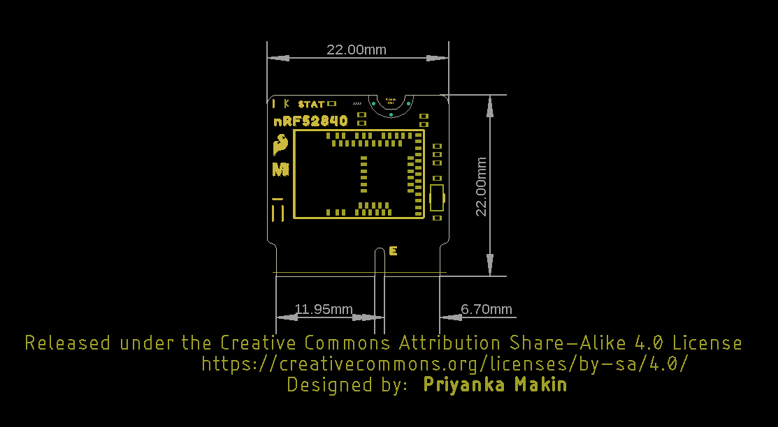
Board Dimensions
MicroMod Processor Boards all measure in at 22mm x 22mm, with 15mm to the top notch and 12mm to the E key. For more information regarding the processor board physical standards, head on over to the Getting Started with MicroMod tutorial and check out the Hardware Overview section.