MicroMod Teensy Processor Hookup Guide
 El Duderino
Hardware Overview
We'll cover the hardware and components included on the MicroMod Teensy Processor Board in this section and highlight some of their unique features.
M.2 Connector
All of our MicroMod Processor come equipped with the M.2 MicroMod Connector, which leverages the M.2 standard and specification to allow you to install your MicroMod Processor on your choice of Carrier Board.
 |
 |
| M.2 Connector from the Front | M.2 Connector from the Back |
The M.2 MicroMod connector is keyed (in tandem with the set screw notch) to prevent the Processor from being inserted and secured improperly.
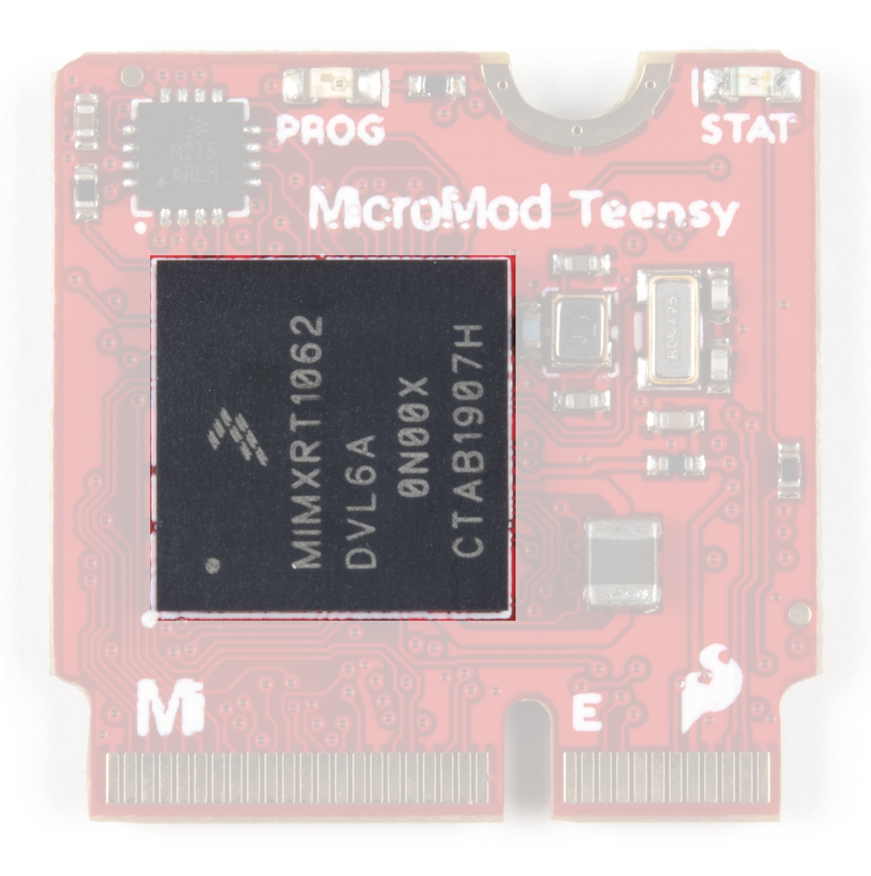
NXP iMXRT1062 Processor
The brain of the MicroMod Teensy Processor is the NXP iMXRT1062 from NXP Semiconductors. This Arm Cortex-M7 core processor is one of the most powerful microprocessors available today. The MicroMod Teensy Processor board takes advantage of the following properties:
- ARM Cortex-M7 at 600MHz
- Seven Serial Ports
- 2 SPI ports (One dedicated SPI available by default on most Carrier Boards[1]. Dedicated Hardware SDIO for SD.)
- 4 I2C Bus (One I2C bus available by default on most Carrier Boards[1])
- USB Host Capability up to 480Mbit/sec making it capable of interfacing with USB flash drives, mice, keyboards and more.
- USB Device Capability up to 480Mbit/sec making it capable of interfacing with USB keyboard/mouse/joystick, MIDI, audio and more.
- 1 CAN Bus Interface
- I2S Digital Audio and S/PDIF
- 12 Dedicated GPIO
- 14 Analog pins (2 dedicated, 10 share signals.)
- 3.3V-tolerant I/O pins
- 16MB Flash Memory (256K reserved for recover & EEPROM emulation)
- 1024K RAM Memory (512K is tightly coupled)
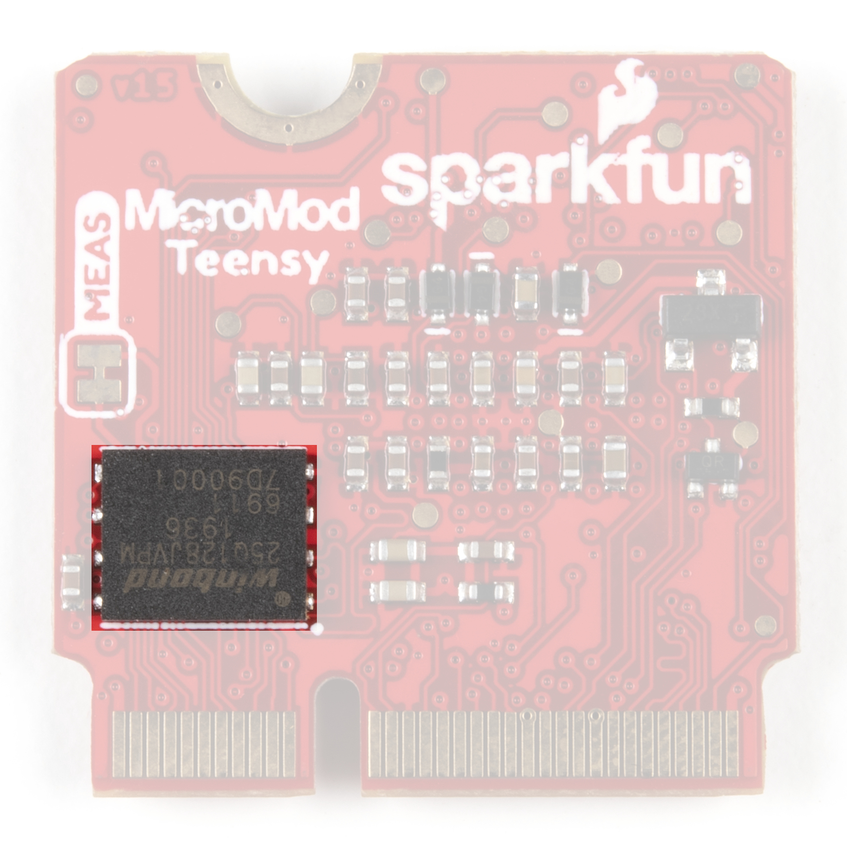
Flash IC
The MicroMod Teensy Processor uses the W25Q128JV-DTR serial flash memory IC from Windbond Electronics. The flash IC features 128mb of memory. For a detailed overview of the IC, refer to the datasheet.
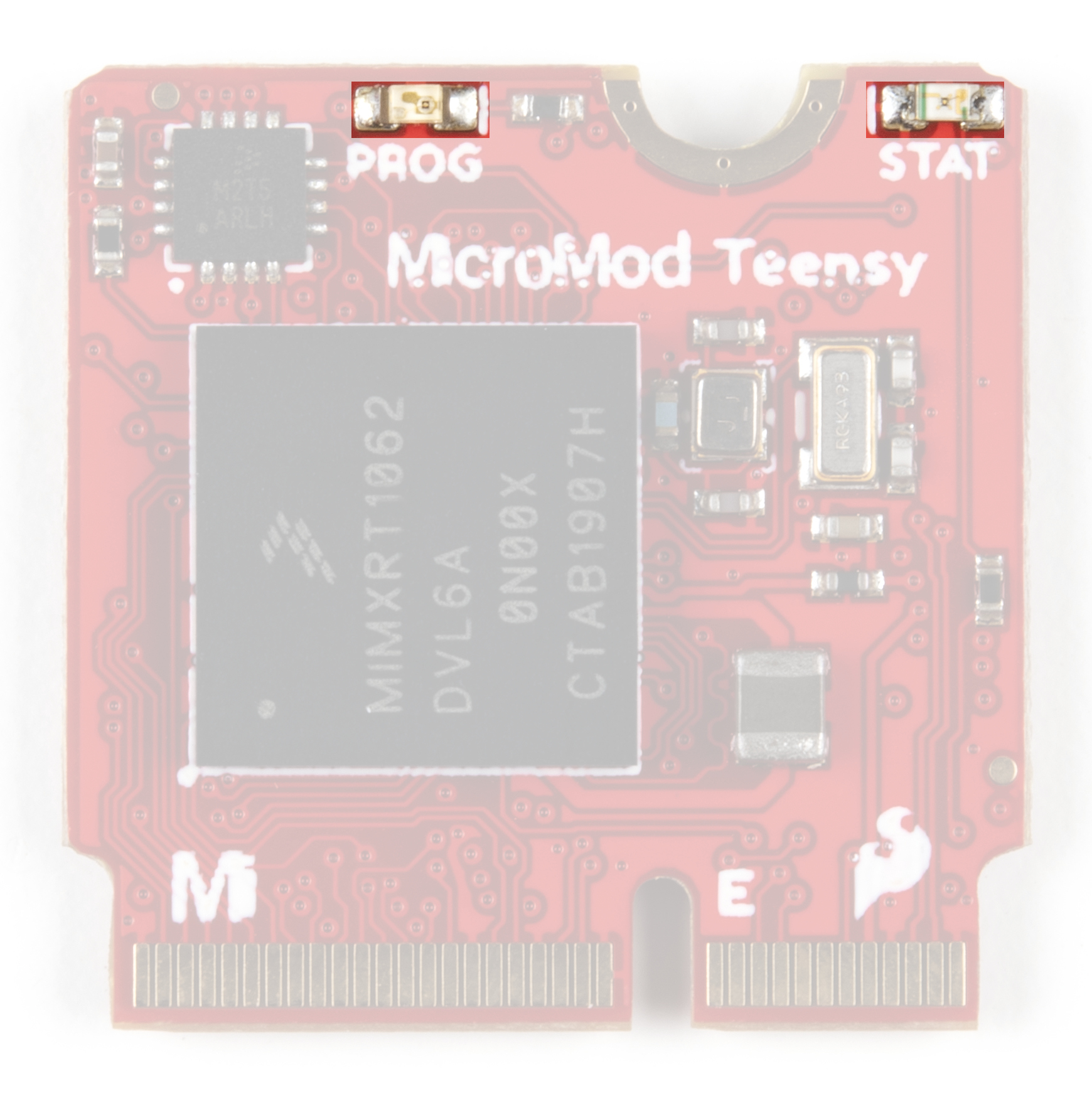
LEDs
There are two LEDs on the Teensy Processor. The PROG LED indicates when the HalfKay bootloader is enabled and the programming IC is powered. We'll cover how to enter the bootloader in the Software Setup and Arduino Example sections. The STAT LED is tied to SCK/13 and can be used as a status LED or as a built-in LED. Control it directly by writing to LED_BUILTIN.
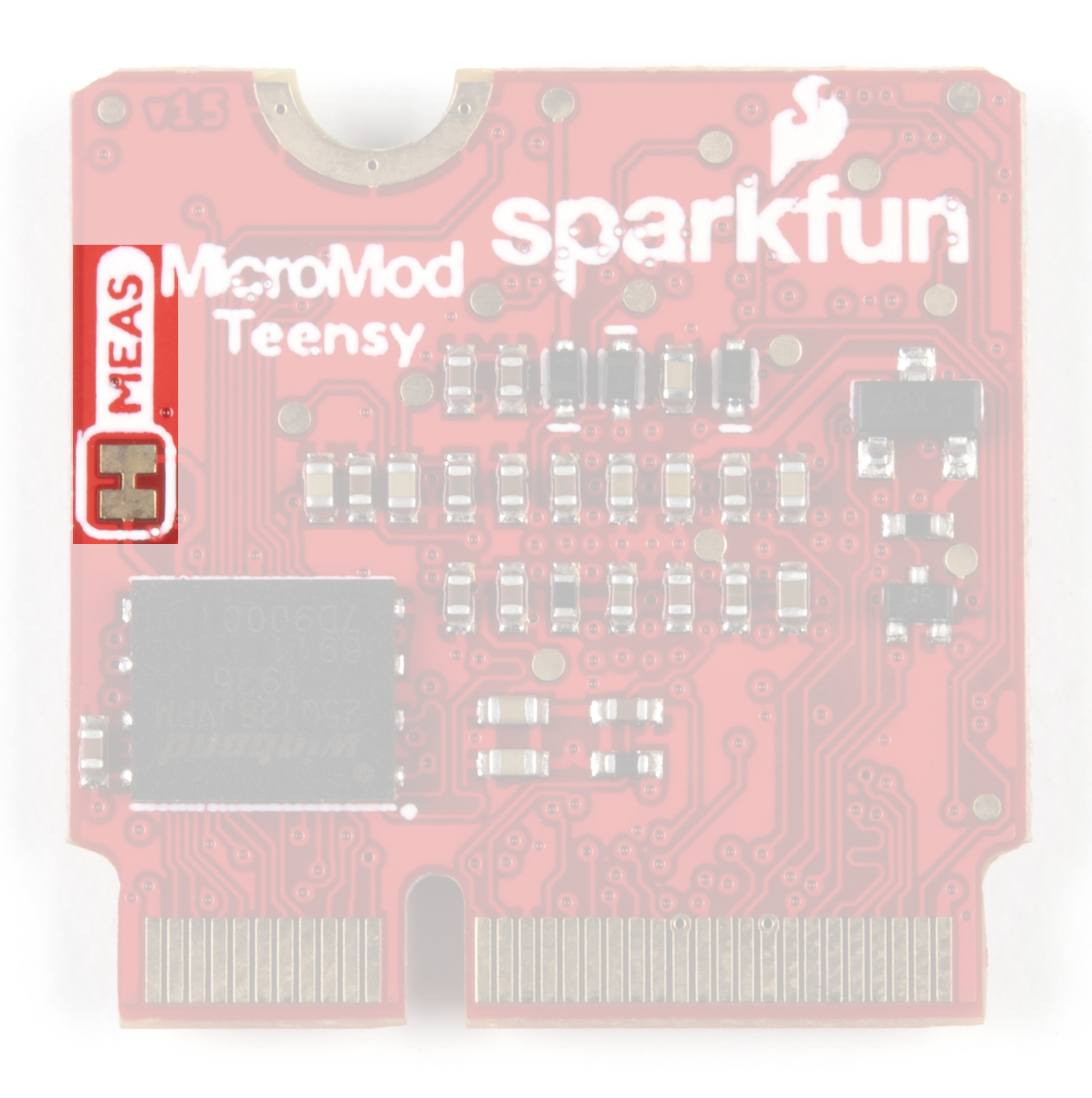
Measure Jumper
The Measure (MEAS) Jumper can be opened to measure how much current the Teensy Processor is pulling from V_USB. It's is CLOSED by default and ties the USB_VBUS pins to V_USB. Open it by severing the trace and then using a digital multimeter to measure the current draw.
Teensy Processor Pin Functions
The Teensy Processor is similar to the Teensy 4.0 and 4.1 with a few notable differences. In order to maintain easy interoperability with MicroMod Carrier Boards, not all of the alternate pin functions are defined for the MicroMod Teensy board variant but we have done our best to make the Teensy Processor as versatile as possible with the right Carrier Board. The sections below outline the various signal protocols available on the MicroMod Teensy.
I2C
As you may have guessed from our extensive Qwiic System, we love communicating with devices using I2C! The Teensy Processor features four I2C buses. The main I2C bus has dedicated pins connected to MiroMod pads 12 (SDA) and 14 (SCL) (Teensy pins 18 and 19), along with a dedicated interrupt pin connected to MicroMod pad 16 (Teensy pin 29). The primary I2C Bus will almost always be connected to a Qwiic connector on your Carrier Board.
If you need a second I2C bus, the Teensy has SDA1 and SCL1 on MicroMod pads 53 and 51 (Teensy pins 25 and 24). To use this second bus, initialize it by calling Wire1.begin();.
UART
The Teensy Processor is capable of having seven UARTs available. The primary UART is tied to USB_D± (MicroMod pads 3 and 5) for serial communication over USB. This is used for your standard serial upload as well as serial prints in Arduino. The secondary UART is a hardware UART tied to MicroMod pads 19 (RX1) and 17 (TX1) (Teensy pins 0 and 1). The tertiary UART is another hardware UART tied to MicroMod pads 20 (RX2) and 22 (TX2) (Teensy pins 17 and 16). In Arduino, the three UARTs are called as listed below:
Serial- Communication over USBSerial1- Communication over RX1/TX1Serial2- Communication over RX2/TX2
SPI
The Teensy Processor has multiple SPI ports. The primary SPI connects to the following pins:
- SDI/CIPO - Serial data input (Controller In/Peripheral Out). MicroMod pad 61. Teensy pin 12.
- SDO/COPI - Serial data output (Controller Out/Peripheral In). MicroMod pad 59. Teensy pin 11.
- SCK - SPI Clock. MicroMod pad 57. Teensy pin 13.
- CS - Chip select. MicroMod pad 55. Teensy pin 10.
SPI Pins: The table below summarizes the SPI objects configured in the Arduino SPI library for the Teensy MicroMod processor board. The numbers in the table correlate with the:
- Pins numbers defined for the Teensy MicroMod processor board in the Arduino IDE
- Pad numbers of the MicroMod connector on a MicroMod processor board
| SPI Pins | Teensy Pin | MicroMod Pad | ||||
|---|---|---|---|---|---|---|
SPI
|
SPI1
|
SPI2
|
SPI
|
SPI1
|
SPI2
|
|
| CIPO | 12 | 1 | 34 | 61 | 17 | 66 |
| COPI | 11 | 26 | 35 | 59 | 67 | 64 |
| SCK | 13 | 27 | 37 | 57 | 8 | 62 |
| CS | 10 | 0 | 36 | 55 | 19 | 60 |
Pin Conflict: In order to prioritize the SDIO functionality of the Teensy processor boards's pin assignment, we had to sacrificed the functionality to the MicroMod connector's SPI1 bus. This was due to the hardware limitations of the microcontroller; since, none of the available SPI buses aligned with the MicroMod connector's SPI1 bus (yellow). With that clarified, please do not confuse the SPI1 bus of the standardized MicroMod connector with SPI1 of the Arduino SPI library.
| MicroMod Connector | Teensy MCU | ||||
|---|---|---|---|---|---|
| Pad | Functions | Functions | Pin | ||
| SPI | SDIO | SDIO | SPI | ||
| 68 |
|
DATA3 | 39 | ||
| 66 | DATA2 | 38 | |||
| 70 | DATA1 | CIPO2 | 34 | ||
| 64 |
|
DATA0 | COPI2 | 35 | |
| 62 |
|
CMD | SCK2 | 37 | |
| 60 |
|
SCK | CS2 | 36 | |
Additionally, some users may recognize that the pins for the SPI2 object are available on the SDIO pads of the MicroMod connector. While the connections don't align with the SPI1 bus of the MicroMod standard, the functionality of SPI2 can be accessed using the Arduino SPI library with carrier boards, where the pins are available (i.e. ATP Carrier Board).
CAN-Bus
One of the unique features of the Teensy is its ability to communicate with CAN devices. The Teensy MicroMod can receive CAN messages but in order to send them properly you will need a separate CAN transceiver. CAN-RX is tied to MicroMod pad 41 (Teensy pin 30) and CAN-TX is tied to MicroMod pad 43 (Teensy pin 31).
AUDIO
The Teensy Processor supports audio using the I2S standard. The pins used are:
- AUD_OUT - GPIO pin 7, pad 56 on the MicroMod, this is the digital audio output.
- AUD_IN - GPIO pin 8, pad 54 on the MicroMod, this is the digital audio input.
- AUD_LRCLK - GPIO pin 20, pad 52 on the MicroMod. Officially called "word select", and also known as "frame sync".
- AUD_BCLK - GPIO pin 21, pad 50 on the MicroMod. Offically called "continuous serial clock, and also known as the "bit clock"
GPIO/BUS
The MicroMod Teensy has all 12 general purpose IO pins available on top of 6 dedicated pins for digital, analog and PWM signals. The dedicated pins are just that, and are not shared with any other pin, unlike the general purpose pins which may be shared with other pins. Take note that not all GPIO pins are broken out or in use on every carrier board. Refer to your Carrier Board's Hookup Guide for more information on pin use.
Dedicated Pins
- A0 - Teensy pin 14, MicroMod pad 34
- A1 - Teensy pin 15, MicroMod pad 38
- D0 - Teensy pin 4, MicroMod pad 10
- D1 - Teensy pin 5, MicroMod pad 18
- PWM0 - Teensy pin 3, MicroMod pad 32
- PWM1 - Teensy pin 2, MicroMod pad 47
General Purpose IO pins
- G0 - Teensy pin 40, MicroMod pad 40
- G1 - Teensy pin 41, MicroMod pad 42
- G2 - Teensy pin 42, MicroMod pad 44
- G3 - Teensy pin 43, MicroMod pad 46
- G4 - Teensy pin 44, MicroMod pad 48
- G5 - Teensy pin 45, MicroMod pad 73
- G6 - Teensy pin 6, MicroMod pad 71
- G7 - Teensy pin 9, MicroMod pad 69
- G8 - Teensy pin 26, MicroMod pad 67
- G9 - Teensy pin 32, MicroMod pad 65
- G10 - Teensy pin 33, MicroMod pad 63
- G11 - Teensy pin 27, MicroMod pad 8
Extra Teensy Functionality
As experienced users may know, the pins on Teensy development boards are very versatile and can be used for a multitude of purposes. As we noted above, in order to maintain compatibility with the rest of the MicroMod system, not all of these alternate functions are available on the MicroMod Teensy but some pins can be configured for things like Analog Inputs or Pulse Width Modulation. As mentioned before, the best way to interact with these pins is with the ATP Carrier Board.
The list below shows all 14 pins on the Teensy Processor available for use as Analog Inputs.
- A0 - Teensy pin 14, dedicated on MM pad 34. PWM-Capable.
- A1 - Teensy pin 15, dedicated on MM pad 38. PWM-Capable.
- A2 - Teensy pin 16, shared with RX2 (MM pad 20). Input Only.
- A3 - Teensy pin 17, shared with TX2 (MM pad 22). Input Only.
- A4 - Teensy pin 18, shared with I2C_SDA (MM pad 12). PWM-Capable.
- A5 - Teensy pin 19, shared with I2C_SCL (MM pad 14). PWM-Capable.
- A6 - Teensy pin 20, shared with AUD_LRCLK (MM pad 52). Input Only.
- A7 - Teensy pin 21, shared with AUD_BCLK (MM pad 50). Input Only.
- A8 - Teensy pin 22, shared with BATT_VIN/3 (MM pad 49). Input Only.
- A9 - Teensy pin 23, shared with AUD_MCLK (MM pad 58). PWM-Capable.
- A10 - Teensy pin 24, shared with I2C_SCL1 (MM pad 53). PWM-Capable.
- A11 - Teensy pin 25, shared with I2C_SDA1 (MM pad 51). PWM-Capable.
- A12 - Teensy pin 26, shared with G8 (MM pad 67). Input Only.
- A13 - Teensy pin 27, shared with G11 (MM pad 8). Input Only.
The default MicroMod Teensy Processor board definition is limited to these extra functionalities along with a few other pins that can technically be used for PWM signals when not in use for other signal protocols. Keep reading to the next section, MicroMod Pinout, for specific information on these pins.
MicroMod Pinout
Refer to the datasheet and user manual for a full overview of the iMXRT1062's capabilities. The complete pin map can be found in the table below or you can refer to the schematic. PJRC has a wealth of knowledge on their forums with regard to the beta testing of the MicroMod Teensy. Here is a specific post that goes into detail about the pin map.
Heads up! The pin table below and schematic both include the Teensy pin associated with each MicroMod pin and this correlation can be used to identify alternate uses for pins on the Teensy Processor but not all of the alternate Teensy functionalities are available for use with the SparkFun Teensy MicroMod board definition. For many of the General Purpose I/O pins and other pins with multiple signal options, refer to your Carrier Board's Hookup Guide for information on how those pins are configured what they are used for. Not all pins are used on every Carrier Board.
Update: Please use the latest version of the Teensy Arduino core, when referencing this table. There have been some small updates to the pin definitions.
| Teensy Arduino Core | Schematic | ||||
|---|---|---|---|---|---|
| v1.54 to 1.55 | ≥ v1.56 | Teensy MCU | MicroMod | ||
| Pin | Pin | Ball | Grid | Pad | Label |
39
|
38
|
SD_B0_04
|
68
|
SDIO_DATA2
|
|
38
|
39
|
SD_B0_05
|
70
|
SPI_CS1/SDIO_DATA3
|
|
*There was an error in the original Teensy 4.0 circuit diagram, which has been fixed in the Teensy Arduino core.
| AUDIO | UART | GPIO/BUS | I2C | SDIO | SPI | Dedicated |
| Teensy Pin | Alternate Function | Primary Function | Bottom Pin |
Top Pin |
Primary Function | Alternate Function | Teensy Pin |
|---|---|---|---|---|---|---|---|
| (Not Connected) | 75 | GND | |||||
| 3.3V | 74 | 73 | G5 | 45 | |||
| RTC_3V_BATT | 72 | 71 | G6 | PWM | 6 | ||
| 39 | SDIO_DATA3 | 70 | 69 | G7 | PWM | 9 | |
| 38 | SDIO_DATA2 | 68 | 67 | G8 | A12 (Input only) | 26 | |
| 34 | SDIO_DATA1 | 66 | 65 | G9 | 32 | ||
| 35 | SDIO_DATA0 | 64 | 63 | G10 | PWM | 33 | |
| 37 | SDIO_CMD | 62 | 61 | SPI_CIPO | PWM | 12 | |
| 36 | SDIO_SCK | 60 | 59 | SPI_COPI | PWM | 11 | |
| 23 | A9 (PWM) | AUD_MCLK | 58 | 57 | SPI_SCK | STAT LED / PWM | 13 |
| 7 | PWM | AUD_OUT | 56 | 55 | SPI_CS | PWM | 10 |
| 8 | PWM | AUD_IN | 54 | 53 | I2C_SCL1 | A10 (PWM) | 24 |
| 20 | A6 (Input Only) | AUD_LRCLK | 52 | 51 | I2C_SDA1 | A11 (PWM) | 25 |
| 21 | A7 (Input Only) | AUD_BCLK | 50 | 49 | BATT_VIN / 3 (0 to 3.3V) | A8 (Input Only) | 22 |
| 44 | G4 | 48 | 47 | PWM1 | 2 | ||
| 43 | G3 | 46 | 45 | GND | |||
| 42 | G2 | 44 | 43 | CAN_TX | 31 | ||
| 41 | G1 | 42 | 41 | CAN_RX | 30 | ||
| 40 | G0 | 40 | 39 | GND | |||
| 15 | PWM | A1 | 38 | 37 | USBHOST_D- | USB2_D- | |
| GND | 36 | 35 | USBHOST_D+ | USB2_D+ | |||
| 14 | PWM | A0 | 34 | 33 | GND | ||
| 3 | PWM0 | 32 | 31 | Module Key | |||
| Module Key | 30 | 29 | Module Key | ||||
| Module Key | 28 | 27 | Module Key | ||||
| Module Key | 26 | 25 | Module Key | ||||
| Module Key | 24 | 23 | Not Connected | ||||
| 17 | A3 (Input Only) | UART_TX2 | 22 | 21 | Not Connected | ||
| 16 | A2 (Input Only) | UART_RX2 | 20 | 19 | UART_RX1 | 0 | |
| 5 | PWM | D1 | 18 | 17 | UART_TX1 | PWM | 1 |
| 29 | PWM | I2C_INT | 16 | 15 | Not Connected | ||
| 19 | A5 (PWM) | I2C_SCL | 14 | 13 | Not Connected | ||
| 18 | A4 (PWM) | I2C_SDA | 12 | 11 | BOOT (Open Drain) | PROG | |
| 4 | PWM | D0 | 10 | 9 | USB_VIN | V_USB | |
| 27 | A13 (Input Only) | G11 | 8 | 7 | GND | ||
| ON/OFF | RESET# (Open Drain) | 6 | 5 | USB_D- | USB_D- | ||
| 28 | 3.3V_EN | 4 | 3 | USB_D+ | USB_D+ | ||
| 3.3V | 2 | 1 | GND |
| Function | Bottom Pin |
Top Pin |
Function | ||||||
|---|---|---|---|---|---|---|---|---|---|
| (Not Connected) | 75 | GND | |||||||
| 3.3V | 74 | 73 | G5 / BUS5 | ||||||
| RTC_3V_BATT | 72 | 71 | G6 / BUS6 | ||||||
| SPI_CS1# | SDIO_DATA3 (I/O) | 70 | 69 | G7 / BUS7 | |||||
| SDIO_DATA2 (I/O) | 68 | 67 | G8 | ||||||
| SDIO_DATA1 (I/O) | 66 | 65 | G9 | ADC_D- | CAM_HSYNC | ||||
| SPI_CIPO1 | SDIO_DATA0 (I/O) | 64 | 63 | G10 | ADC_D+ | CAM_VSYNC | |||
| SPI COPI1 | SDIO_CMD (I/O) | 62 | 61 | SPI_CIPO (I) | |||||
| SPI SCK1 | SDIO_SCK (O) | 60 | 59 | SPI_COPI (O) | LED_DAT | ||||
| AUD_MCLK (O) | 58 | 57 | SPI_SCK (O) | LED_CLK | |||||
| CAM_MCLK | PCM_OUT | I2S_OUT | AUD_OUT | 56 | 55 | SPI_CS# | |||
| CAM_PCLK | PCM_IN | I2S_IN | AUD_IN | 54 | 53 | I2C_SCL1 (I/O) | |||
| PDM_DATA | PCM_SYNC | I2S_WS | AUD_LRCLK | 52 | 51 | I2C_SDA1 (I/O) | |||
| PDM_CLK | PCM_CLK | I2S_SCK | AUD_BCLK | 50 | 49 | BATT_VIN / 3 (I - ADC) (0 to 3.3V) | |||
| G4 / BUS4 | 48 | 47 | PWM1 | ||||||
| G3 / BUS3 | 46 | 45 | GND | ||||||
| G2 / BUS2 | 44 | 43 | CAN_TX | ||||||
| G1 / BUS1 | 42 | 41 | CAN_RX | ||||||
| G0 / BUS0 | 40 | 39 | GND | ||||||
| A1 | 38 | 37 | USBHOST_D- | ||||||
| GND | 36 | 35 | USBHOST_D+ | ||||||
| A0 | 34 | 33 | GND | ||||||
| PWM0 | 32 | 31 | Module Key | ||||||
| Module Key | 30 | 29 | Module Key | ||||||
| Module Key | 28 | 27 | Module Key | ||||||
| Module Key | 26 | 25 | Module Key | ||||||
| Module Key | 24 | 23 | SWDIO | ||||||
| UART_TX2 (O) | 22 | 21 | SWDCK | ||||||
| UART_RX2 (I) | 20 | 19 | UART_RX1 (I) | ||||||
| CAM_TRIG | D1 | 18 | 17 | UART_TX1 (0) | |||||
| I2C_INT# | 16 | 15 | UART_CTS1 (I) | ||||||
| I2C_SCL (I/0) | 14 | 13 | UART_RTS1 (O) | ||||||
| I2C_SDA (I/0) | 12 | 11 | BOOT (I - Open Drain) | ||||||
| D0 | 10 | 9 | USB_VIN | ||||||
| SWO | G11 | 8 | 7 | GND | |||||
| RESET# (I - Open Drain) | 6 | 5 | USB_D- | ||||||
| 3.3V_EN | 4 | 3 | USB_D+ | ||||||
| 3.3V | 2 | 1 | GND | ||||||
| Signal Group | Signal | I/O | Description | Voltage | Power | 3.3V | I | 3.3V Source | 3.3V |
|---|---|---|---|---|
| GND | Return current path | 0V | ||
| USB_VIN | I | USB VIN compliant to USB 2.0 specification. Connect to pins on processor board that require 5V for USB functionality | 4.8-5.2V | |
| RTC_3V_BATT | I | 3V provided by external coin cell or mini battery. Max draw=100μA. Connect to pins maintaining an RTC during power loss. Can be left NC. | 3V | |
| 3.3V_EN | O | Controls the carrier board's main voltage regulator. Voltage above 1V will enable 3.3V power path. | 3.3V | |
| BATT_VIN/3 | I | Carrier board raw voltage over 3. 1/3 resistor divider is implemented on carrier board. Amplify the analog signal as needed for full 0-3.3V range | 3.3V | |
| Reset | Reset | I | Input to processor. Open drain with pullup on processor board. Pulling low resets processor. | 3.3V |
| Boot | I | Input to processor. Open drain with pullup on processor board. Pulling low puts processor into special boot mode. Can be left NC. | 3.3V | |
| USB | USB_D± | I/O | USB Data ±. Differential serial data interface compliant to USB 2.0 specification. If UART is required for programming, USB± must be routed to a USB-to-serial conversion IC on the processor board. | |
| USB Host | USBHOST_D± | I/O | For processors that support USB Host Mode. USB Data±. Differential serial data interface compliant to USB 2.0 specification. Can be left NC. | |
| CAN | CAN_RX | I | CAN Bus receive data. | 3.3V |
| CAN_TX | O | CAN Bus transmit data. | 3.3V | |
| UART | UART_RX1 | I | UART receive data. | 3.3V |
| UART_TX1 | O | UART transmit data. | 3.3V | |
| UART_RTS1 | O | UART request to send. | 3.3V | |
| UART_CTS1 | I | UART clear to send. | 3.3V | |
| UART_RX2 | I | 2nd UART receive data. | 3.3V | |
| UART_TX2 | O | 2nd UART transmit data. | 3.3V | |
| I2C | I2C_SCL | I/O | I2C clock. Open drain with pullup on carrier board. | 3.3V |
| I2C_SDA | I/O | I2C data. Open drain with pullup on carrier board | 3.3V | |
| I2C_INT# | I | Interrupt notification from carrier board to processor. Open drain with pullup on carrier board. Active LOW | 3.3V | |
| I2C_SCL1 | I/O | 2nd I2C clock. Open drain with pullup on carrier board. | 3.3V | |
| I2C_SDA1 | I/O | 2nd I2C data. Open drain with pullup on carrier board. | 3.3V | |
| SPI | SPI_COPI | O | SPI Controller Output/Peripheral Input. | 3.3V |
| SPI_CIPO | I | SPI Controller Input/Peripheral Output. | 3.3V | |
| SPI_SCK | O | SPI Clock. | 3.3V | |
| SPI_CS# | O | SPI Chip Select. Active LOW. Can be routed to GPIO if hardware CS is unused. | 3.3V | |
| SPI/SDIO | SPI_SCK1/SDIO_CLK | O | 2nd SPI Clock. Secondary use is SDIO Clock. | 3.3V |
| SPI_COPI1/SDIO_CMD | I/O | 2nd SPI Controller Output/Peripheral Input. Secondary use is SDIO command interface. | 3.3V | |
| SPI_CIPO1/SDIO_DATA0 | I/O | 2nd SPI Peripheral Input/Controller Output. Secondary use is SDIO data exchange bit 0. | 3.3V | |
| SDIO_DATA1 | I/O | SDIO data exchange bit 1. | 3.3V | |
| SDIO_DATA2 | I/O | SDIO data exchange bit 2. | 3.3V | |
| SPI_CS1/SDIO_DATA3 | I/O | 2nd SPI Chip Select. Secondary use is SDIO data exchange bit 3. | 3.3V | |
| Audio | AUD_MCLK | O | Audio master clock. | 3.3V |
| AUD_OUT/PCM_OUT/I2S_OUT/CAM_MCLK | O | Audio data output. PCM synchronous data output. I2S serial data out. Camera master clock. | 3.3V | |
| AUD_IN/PCM_IN/I2S_IN/CAM_PCLK | I | Audio data input. PCM syncrhonous data input. I2S serial data in. Camera periphperal clock. | 3.3V | |
| AUD_LRCLK/PCM_SYNC/I2S_WS/PDM_DATA | I/O | Audio left/right clock. PCM syncrhonous data SYNC. I2S word select. PDM data. | 3.3V | |
| AUD_BCLK/PCM_CLK/I2S_CLK/PDM_CLK | O | Audio bit clock. PCM clock. I2S continuous serial clock. PDM clock. | 3.3V | |
| SWD | SWDIO | I/O | Serial Wire Debug I/O. Connect if processor board supports SWD. Can be left NC. | 3.3V |
| SWDCK | I | Serial Wire Debug clock. Connect if processor board supports SWD. Can be left NC. | 3.3V | |
| ADC | A0 | I | Analog to digital converter 0. Amplify the analog signal as needed to enable full 0-3.3V range. | 3.3V |
| A1 | I | Analog to digital converter 1. Amplify the analog signal as needed to enable full 0-3.3V range. | 3.3V | |
| PWM | PWM0 | O | Pulse width modulated output 0. | 3.3V |
| PWM1 | O | Pulse width modulated output 1. | 3.3V | |
| Digital | D0 | I/O | General digital input/output pin. | 3.3V |
| D1/CAM_TRIG | I/O | General digital input/output pin. Camera trigger. | 3.3V | |
| General/Bus | G0/BUS0 | I/O | General purpose pins. Any unused processor pins should be assigned to Gx with ADC + PWM capable pins given priority (0, 1, 2, etc.) positions. The intent is to guarantee PWM, ADC and Digital Pin functionality on respective ADC/PWM/Digital pins. Gx pins do not guarantee ADC/PWM function. Alternative use is pins can support a fast read/write 8-bit or 4-bit wide bus. | 3.3V |
| G1/BUS1 | I/O | 3.3V | ||
| G2/BUS2 | I/O | 3.3V | ||
| G3/BUS3 | I/O | 3.3V | ||
| G4/BUS4 | I/O | 3.3V | ||
| G5/BUS5 | I/O | 3.3V | ||
| G6/BUS6 | I/O | 3.3V | ||
| G7/BUS7 | I/O | 3.3V | ||
| G8 | I/O | General purpose pin | 3.3V | |
| G9/ADC_D-/CAM_HSYNC | I/O | Differential ADC input if available. Camera horizontal sync. | 3.3V | |
| G10/ADC_D+/CAM_VSYNC | I/O | Differential ADC input if available. Camera vertical sync. | 3.3V | |
| G11/SWO | I/O | General purpose pin. Serial Wire Output | 3.3V |
Board Dimensions
MicroMod Processors all measure in at 22mm x 22mm, with 15mm to the top notch and 12mm to the E key. For more information regarding the processor board physical standards, head on over to the Getting Started with MicroMod and Designing With MicroMod tutorials.
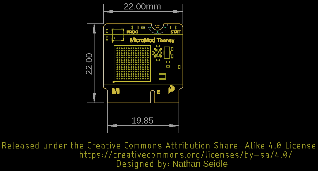
The overall thickness of the MicroMod Teensy Processor Board is ~3.10mm. The height of the tallest component (NXP iMXRT1062 labeled as "U1" in the board file) on the Processor side is ~1.28mm. The PCB thickness is ~0.80mm. The height of the tallest component (transistor labeled as "Q1" in the board file) is about ~1.02mm.