MPU-9250 Hookup Guide
 .Brent.
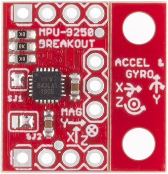
 Board Overview
 PCB" />
The board is designed to be smaller than some of our other offerings to fit in smaller projects. To achieve this, the PTHs are wrapped around the boarder of the PCB in three rows of three or four. The top row (J1) is all one need to get most of the functionality of the IMU. These include the I2C and power interface. If space were really tight, one could take a saw and carefully remove all of the other PTHs.
The second most likely to be used set of PTHs are found along the bottom (J3). This includes the address pin, the interrupt pin, and the IO voltage supply for easy interface with a more modern 1.8V processor.
The third, non-breadboard-compatible row (J2) is used for features like running other I2C devices as slaves to this one. For prototyping with these connections, throw your connections on top like you would with an Arduino Pro Mini or similar product.
PTH Connections
The following table summarizes all of the plated through hole (PTH) connections on the breakout board in order found on the board stating in the upper-left corner and wrapping clockwise:
| Pin Label | Pin Function | Notes |
|---|---|---|
| SCL | I2C serial clock SPI serial port clock | 100 or 400 kHz I2C Up to 1 MHz SPI (20 MHz in certain cases) |
| SDA | I2C serial data | Can also be used for SPI serial data input (SDI) |
| VDD | Power supply | +2.4V to +3.6V |
| GND | Ground reference | +0V |
| AUXDA | Ground reference | I2C master serial data, for connecting to external sensors |
| FSYNC | Ground reference | Frame synchronization digital input. Connect to GND if unused. |
| AUXCL | Ground reference | I2C Master serial clock, for connecting to external sensors |
| INT | Interrupt signal | Interrupt digital output (totem pole or open-drain) |
| CS | Chip select | Chip select (SPI mode only) |
| AD0/ SDO | Address selection | I2C Slave Address LSB (AD0): Low: 0b1101000 ➫ 0x68 High: 0b1101001 ➫ 0x69 SPI serial data output (SDO) |
| VDDIO | Power supply for I/O pins | +1.71V up to VDD |
Jumpers
The MPU-9250 Breakout has two solder jumpers, SJ1 and SJ2.
SJ1 comes pre-soldered to short VDD and VDDIO. This reduces the number of power supplies to one with out requiring an external jumper. If the core and IO need to be supplied with different voltages, remove the solder from SJ1.
SJ2 is a two way jumper that comes pre-soldered to connect AD0 to ground. This sets the I2C address to 0x68. It also leaves the PTH for AD0 disconnected and floating. If the solder is moved to connect the center pad with the pad on the left, then the AD0 PTH needs to be connected high or low to chose the I2C address.
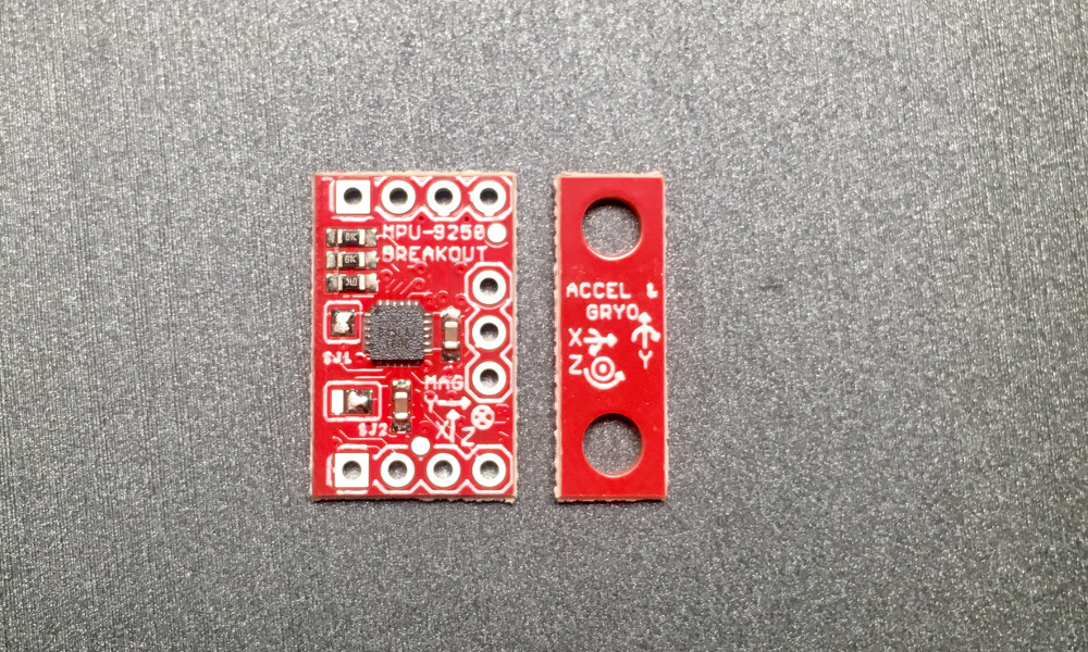
Reducing size
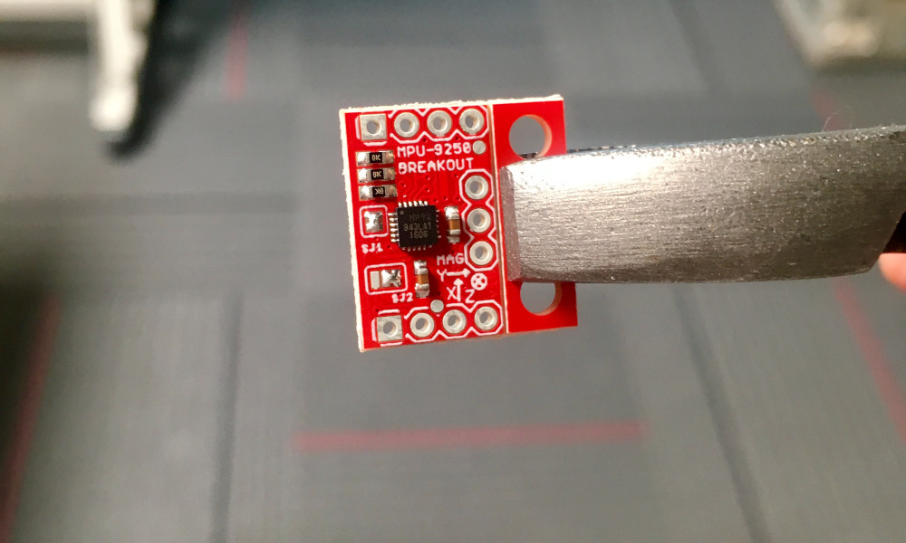
As stated earlier, one of the design goals for this breakout was to make the board small. Some projects will require mounting holes, so we threw them on the right side of some v-score on this board. Since the board is only ⅔" wide and there isn't enough mass to the left of the mounting holes, there isn't much of a bending moment.
If you plan to use a breadboard, or secure the IMU securely to a project with something like epoxy, the mounting holes can be snapped off. As shown in the following image. The pliers I had on hand made super easy work of this. The edge of a table should work fine too.