PCB Basics
 SFUptownMaker
Composition
A PCB is sort of like a layer cake or lasagna- there are alternating layers of different materials which are laminated together with heat and adhesive such that the result is a single object.
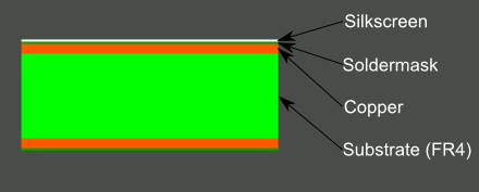
Let's start in the middle and work our way out.
FR4
The base material, or substrate, is usually fiberglass. Historically, the most common designator for this fiberglass is "FR4". This solid core gives the PCB its rigidity and thickness. There are also flexible PCBs built on flexible high-temperature plastic (Kapton or the equivalent).
You will find many different thickness PCBs; the most common thickness for SparkFun products is 1.6mm (0.063"). Some of our products- LilyPad boards and Arudino Pro Micro boards- use a 0.8mm thick board.
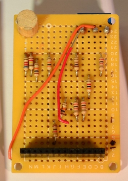
Cheaper PCBs and perf boards (shown above) will be made with other materials such as epoxies or phenolics which lack the durability of FR4 but are much less expensive. You will know you are working with this type of PCB when you solder to it - they have a very distictive bad smell. These types of substrates are also typically found in low-end consumer electronics. Phenolics have a low thermal decomposition temperature which causes them to delaminate, smoke and char when the soldering iron is held too long on the board.
Copper
The next layer is a thin copper foil, which is laminated to the board with heat and adhesive. On common, double sided PCBs, copper is applied to both sides of the substrate. In lower cost electronic gadgets the PCB may have copper on only one side. When we refer to a double sided or 2-layer board we are referring to the number of copper layers (2) in our lasagna. This can be as few as 1 layer or as many as 16 layers or more.
The copper thickness can vary and is specified by weight, in ounces per square foot. The vast majority of PCBs have 1 ounce of copper per square foot but some PCBs that handle very high power may use 2 or 3 ounce copper. Each ounce per square translates to about 35 micrometers or 1.4 thousandths of an inch of thickness of copper.
Soldermask
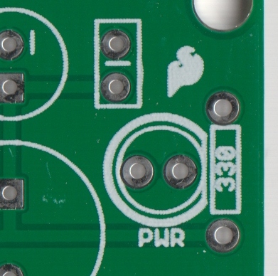
The layer on top of the copper foil is called the soldermask layer. This layer gives the PCB its green (or, at SparkFun, red) color. It is overlaid onto the copper layer to insulate the copper traces from accidental contact with other metal, solder, or conductive bits. This layer helps the user to solder to the correct places and prevent solder jumpers.
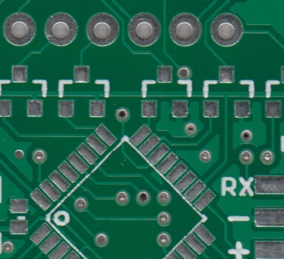
In the example below, the green solder mask is applied to the majority of the PCB, covering up the small traces but leaving the silver rings and SMD pads exposed so they can be soldered to.
Soldermask is most commonly green in color but nearly any color is possible. We use red for almost all the SparkFun boards, white for the IOIO board, and purple for the LilyPad boards.
Silkscreen
The white silkscreen layer is applied on top of the soldermask layer. The silkscreen adds letters, numbers, and symbols to the PCB that allow for easier assembly and indicators for humans to better understand the board. We often use silkscreen labels to indicate what the function of each pin or LED.
Silkscreen is most commonly white but any ink color can be used. Black, gray, red, and even yellow silkscreen colors are widely available; it is, however, uncommon to see more than one color on a single board.