Power Delivery Board - USB-C (Qwiic) Hookup Guide
 Alex the Giant, Ell C
Hardware Overview
STUSB4500
When it comes to power delivery you have two types of power roles. The first is the provider, also known as the source, which is capable of providing power over the USB power bus. The other role is the consumer, also known as the sink, which draws power from the source.
The STUSB4500 is a USB Type-C and power delivery controller IC for sink applications. The controller is able to negotiate a power delivery contract with a source (ie a power delivery wall wart or power adapter) without the need for an external microcontroller, although you will need a microcontroller to configure the board. With this controller, we are taking advantage of STMicroelectronic's proprietary algorithms and configurable power data objects (PDOs) using integrated non-volatile memory (NVM). Its laundry list of features include:
- "Attach detection" between two USB Type-C ports
- Establish a valid source-to-sink connection
- Negotiate a USB power delivery (PD) contract with a PD capable source
- Monitor the VBUS power path and manage the VBUS voltage transitions
- Manage high voltage protections
- Dual high power charging path support
Understanding how the power negotiation will be covered in the USB-C Power Negotiation section, but for right now, let's go over the board itself.
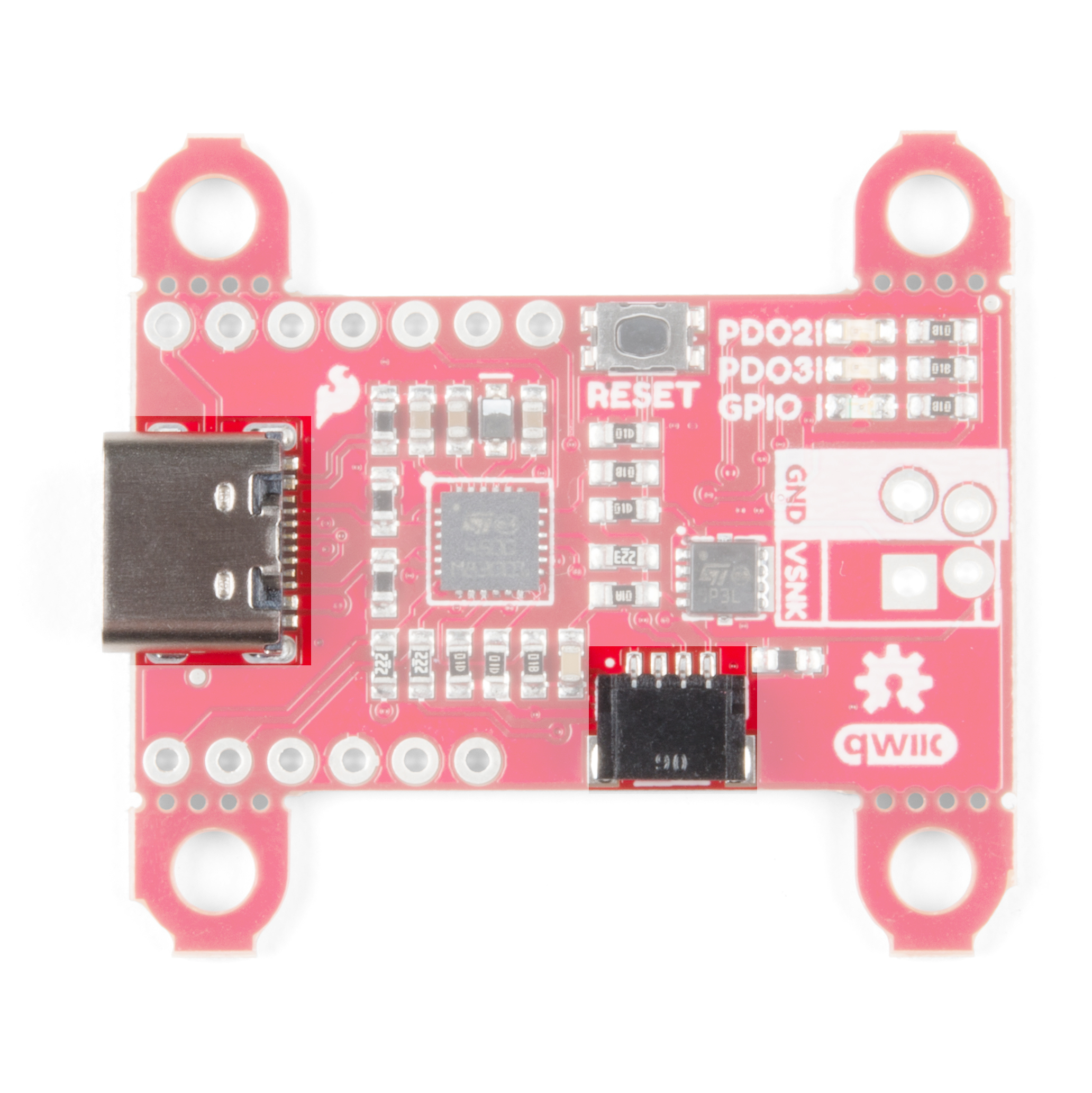
Power
The Power Delivery board can be powered in one of two ways, either through the USB Type-C connector, or with 3.3V from the Qwiic Connector if you just need to configure a new power delivery profile.
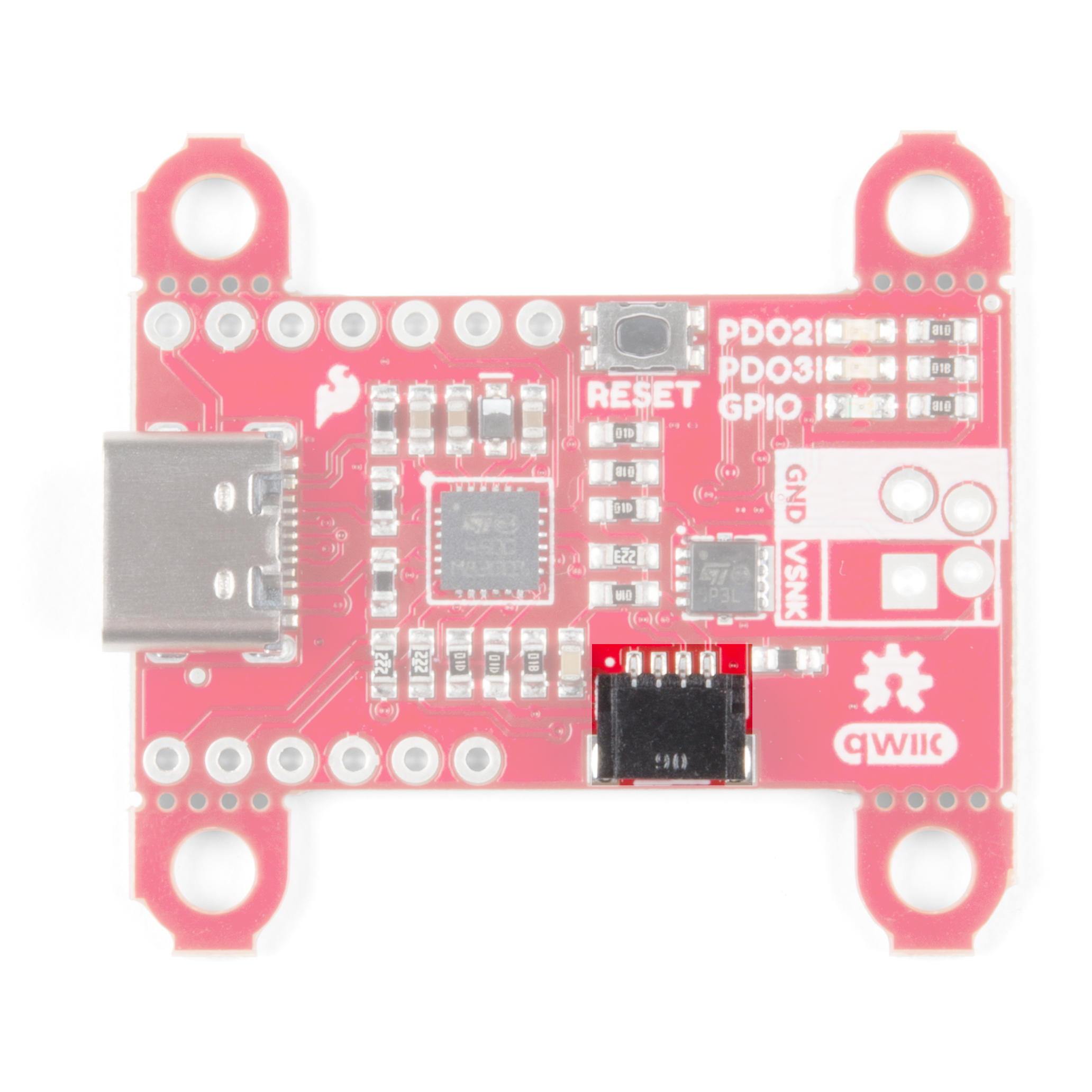
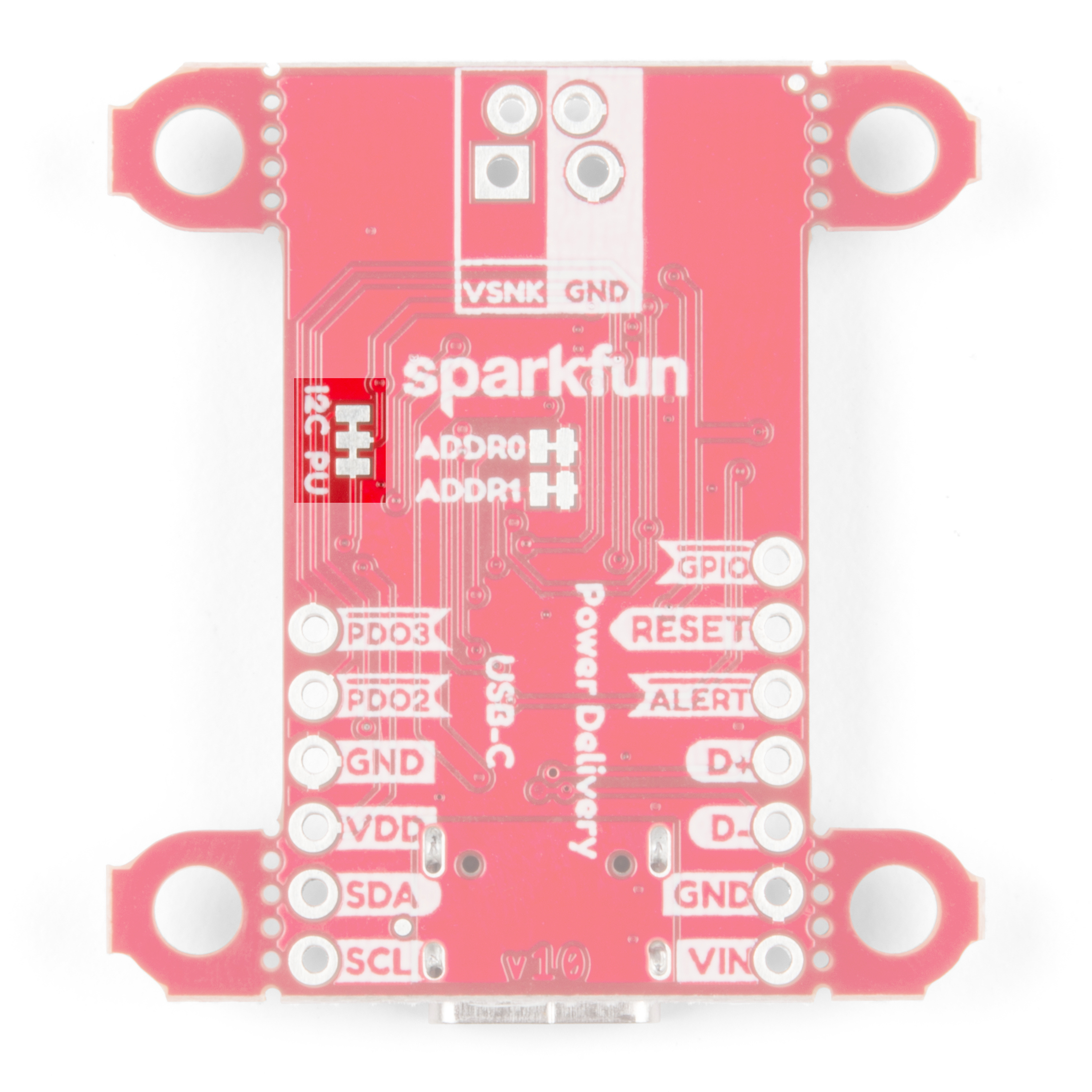
I2C Pins
To configure the board, you will need an I2C bus. The Qwiic system makes it easy to connect the Power Delivery board to a microcontroller to set the NVM parameters to power your project via the Qwiic connector. Depending on your application, you can also connect to the I2C bus via the plated through holes for SDA and SCL.
 |
 |
| Top View | Bottom View |
Pins
The board breaks out the following pins:
| Pin Name | Description |
|---|---|
| VIN | This is the input power pin, which is connected to VBUS on the Type-C connector. |
| VSNK | Power output enabled after successful power negotiation |
| VDD | Optional logic power input, 3.0V - 5.5V |
| GND | Ground |
| SCL | I2C clock input |
| SDA | I2C data input/output |
| D- | USB 2.0 differential pair, negative |
| D+ | USB 2.0 differential pair, positive |
| Alert | I2C interrupt, active low open drain |
| Reset | Reset input, active high |
| GPIO | General purpose output, active low open drain |
| PDO2 | Power contract flag for PDO2, active low open drain |
| PDO3 | Power contract flag for PDO3, active low open drain |

Jumpers
The board has a few jumper pads to configure the I2C bus.
How to Work with Jumper Pads and PCB Traces
April 2, 2018
Address Select
The default address of the board is 0x28. If you need to adjust the address of the board, you can cut one or both of the address pads labels ADDR0 and ADDR1.
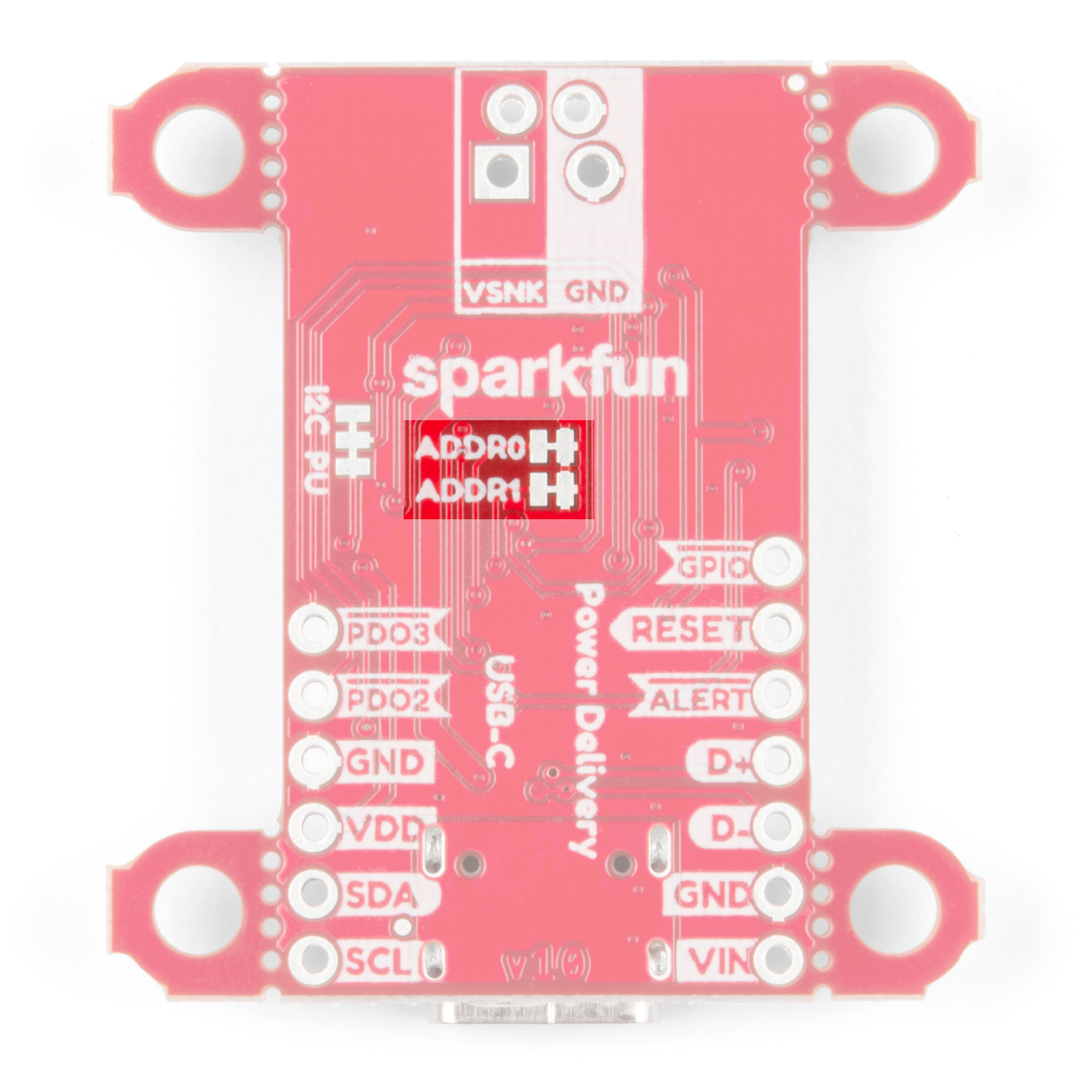
The table below lists the four jumper configurations along with the corresponding hexadecimal device address.
| ADDR0 | ADDR1 | Device Address |
|---|---|---|
| Closed | Closed | 0x28 (default) |
| Open | Closed | 0x29 |
| Closed | Open | 0x2A |
| Open | Open | 0x2B |
Pull-Up Resistors
The board also includes jumpers to disable the pull-up resistors on the I2C bus. If you are using a few I2C devices on the same bus that already have pull-up resistors on their board, you may want to cut the jumpers to disconnect these pull-up resistors. The Power Delivery board utilizes non-volatile memory, the settings saved to device stay configured even if it loses power, so the only time this board needs to be connected over I2C is to modify the NVM parameters.
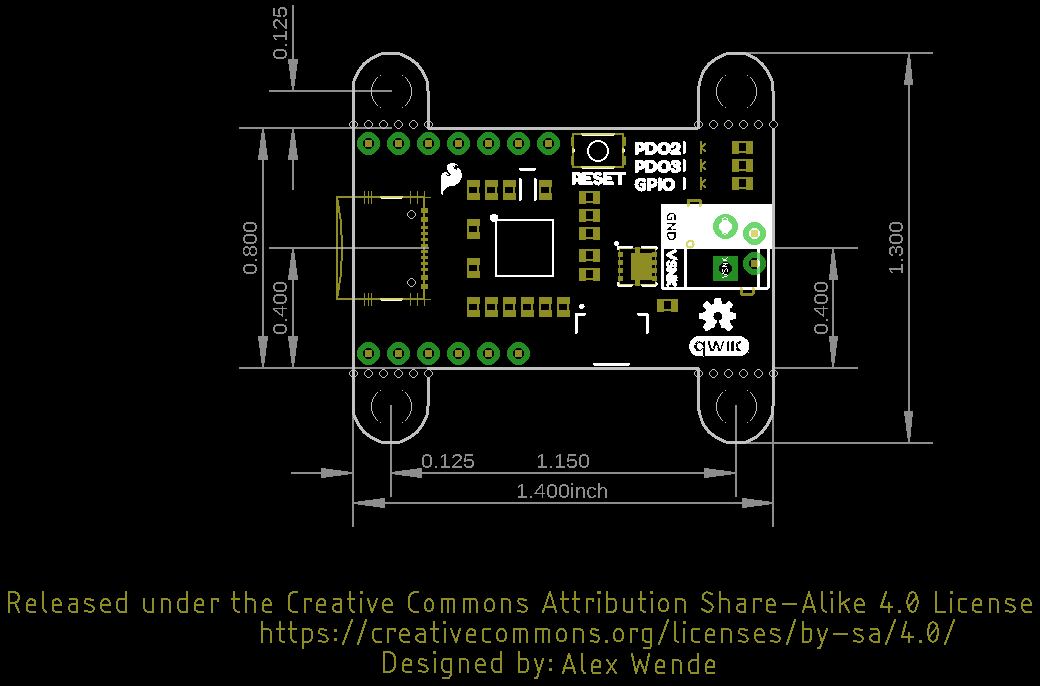
Dimensions