Proto Pedal Assembly and Theory Guide
 Byron J.
Prototyping With The Proto Pedal
While you're developing your circuit, you can place a solderless breadboard over the center of the board.
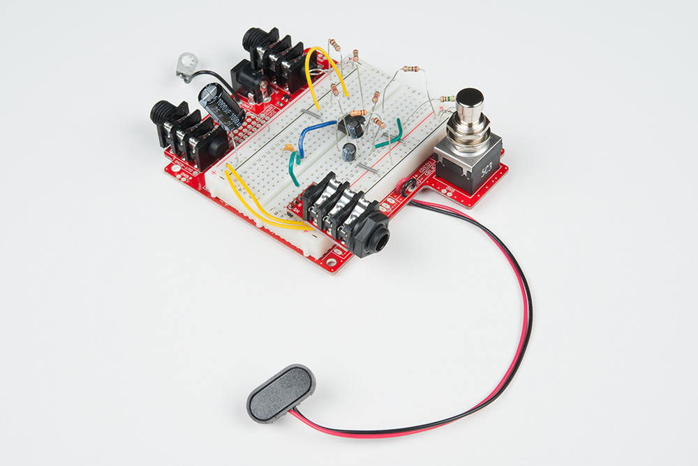
When you're ready to finalize the design, you can transcribe the circuit onto the Proto Pedal PCB. The connections in this area of the PCB duplicate those on the solderless board.
There is one difference between the breadboard and Proto Pedal layout, though. There are two additional side-to-side traces down the center of the proto area.
These traces aren't assigned to any specific signal, but can be easily tied to VCC, GND, or VAUX using the pads at the left edge of the board. We'll discuss VAUX shortly.
Coupling Caps
The input and output to a guitar pedal circuit almost always use coupling capacitors at the input and output. There are footprints for these caps near the lower edge of the PCB.
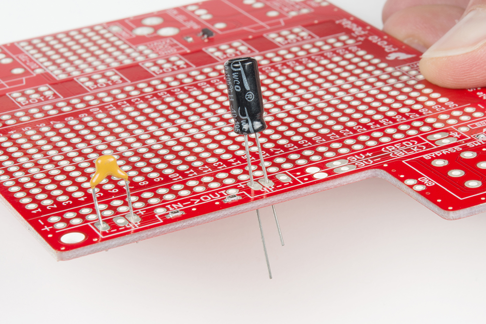
Not every circuit uses the same value, size or composition of capacitor. Therefore, these footprints are designed to accommodate a variety of lead spacing. These locations fit both 2mm and 5mm caps, as shown above.
If you're using polarized coupling caps, the + leads usually face the circuit input/output pads, as marked on the PCB.
Your Circuit Goes Here
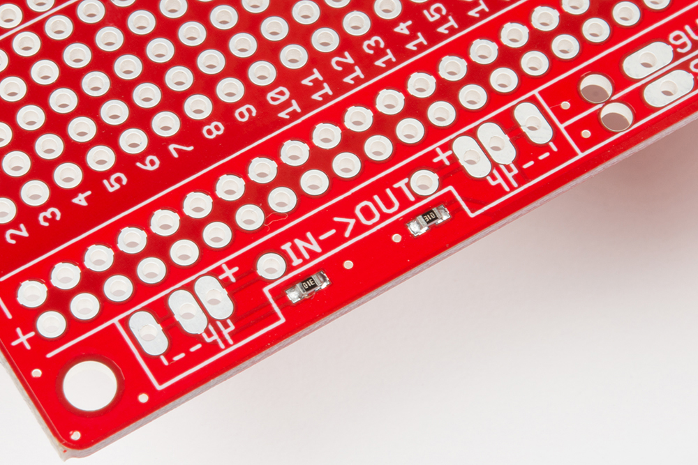
With the coupling caps in place, the input and output to the heart of the circuit are the through-hole pads between the coupling caps, marked IN and OUT.
Adding Knobs
The PCB also has six positions for adding potentiometers.
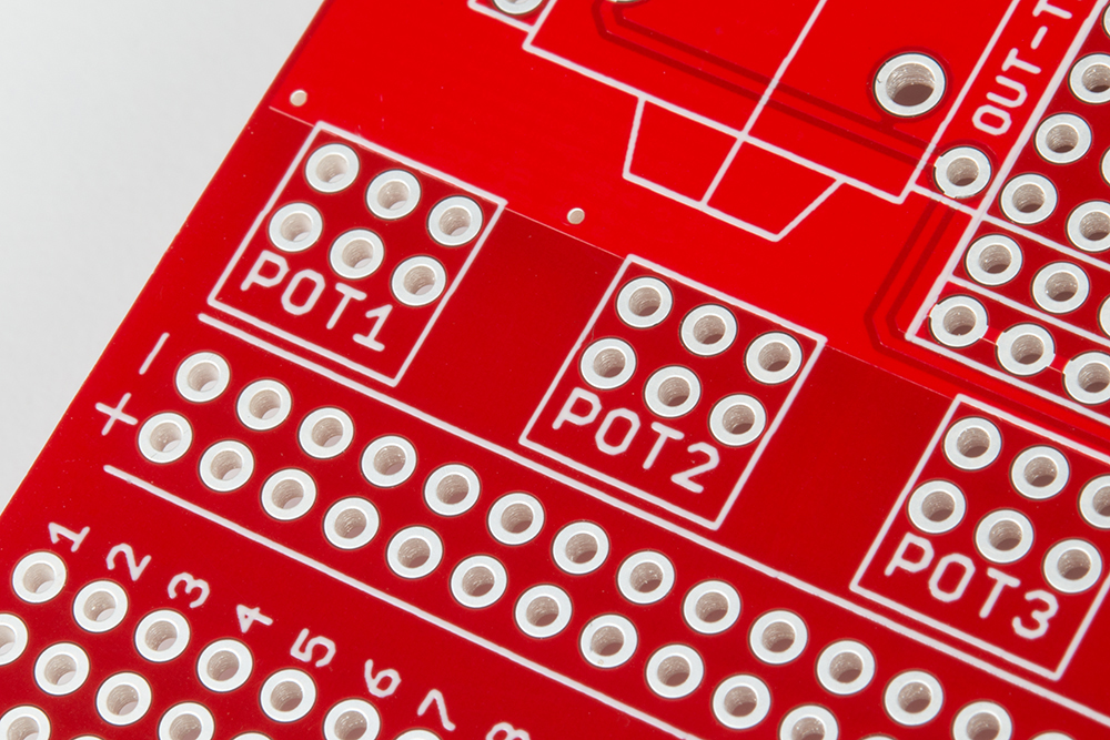
The intent of these positions is that you can run short wires from the proto area to the lower row of pads, then run longer wires from the top pads to the pots, which are bolted to the chassis. This helps keep the proto area tidy.
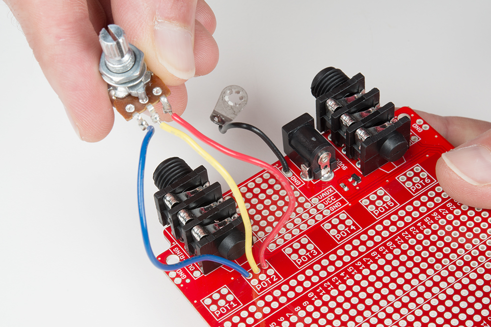
The concept of leaving the wires a little long is known as a "Service Loop" -- the system can be disassembled and the PCB can be accessed without having to take the pots off the front panel or disconnect any wires.
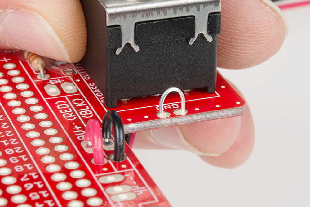
Power Supply Area
There is an extra pad-per-hole proto area between the TRS jacks. This area is intended to allow you to add extra circuitry, such as a voltage regulator or rail splitter. If you're really ambitious, you could build a charge pump circuit in this area, to generate bipolar power supply rails.
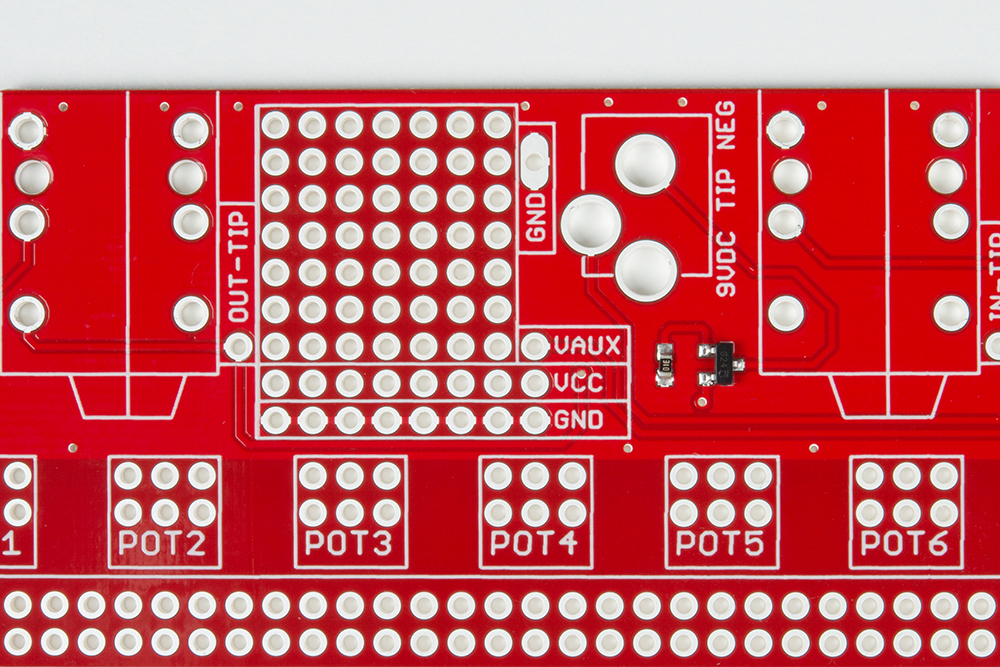
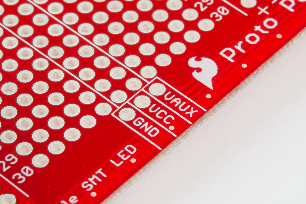
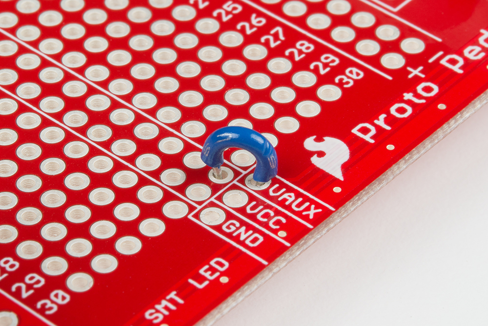
If you're deriving a new voltage rail, there is also an uncommitted trace from this area to the proto area, marked VAUX, for "auxillary voltage."
The three connections at the lower left of this area (VAUX,VCC,GND) run to the similarly named set of pads to the right of the prototyping area.
Prototyping Area
The center of the board is the same as a medium-sized solderless breadboard.
Across the top and bottom of this area are power supply traces that run from side to side. The Trace marked + is tied to VCC, and the trace marked - is tied to ground. Between the power traces are pairs of five-pad vertical groupings, arranged in 30 columns. Typically, a dual-in-line (DIP) IC package is placed so it spans the gap at the center of the board.
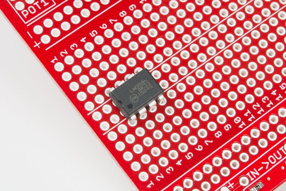
Each leg of the IC is then electrically continuous with the remaining four holes in the group. A short wire can be used as a jumper to connect pads to the power rails, and passive components like capacitors and resistors can be inserted between rows to make connections.
Extra Lateral Traces
On an ordinary DIP-IC prototyping board, the space down the center of the proto area (between the two sets of pads) is empty. The Proto Pedal has an extra pair of traces running in this area.
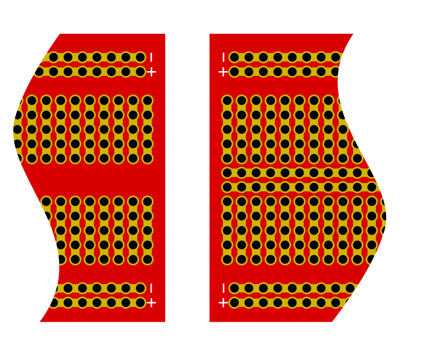
These traces simply run from left to right -- you can decide how they're used in your design. For convenience, VCC, Ground and VAUX can be found on pads near the right end of these traces and can be jumpered to the center traces.
We'll show an example that uses these traces in the EQ Pedal project.
Ground Lugs and Test Points
There are a number of extra through hole pads on the PCB. There are several pairs of ground pads, which can be populated with small wire loops so you can clip a multimeter or oscilloscope probe ground to them.
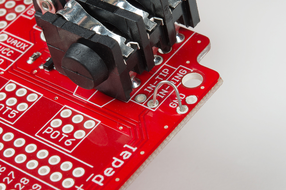
There are also test points providing access to the tip and ring of the input and output, adjacent to their respective jacks. The ring of the input jack can be found near the ground connection at the top-right corner of the board -- if you need to power the pedal even when the input jack is unplugged, you can run a piece of wire between them. Just don't forget to remove it before deploying the pedal, or your battery life will suffer!
It Reads From Right-To-Left
When seen from the user's perspective, the Proto Pedal is on the floor near their feet, with the stomp switch facing towards them and the jacks facing away.
In another puzzling but long-standing FX pedal convention, viewed this way, the input jack is on the right and the output is on the left. One plausible explanation for this is that the cable usually comes out of the guitar towards the right, so it doesn't have to cross back to the left to get plugged in.
This is the opposite of how we typically think about circuits and draw schematics (with signal flowing from left-to-right). It's just a detail to keep in mind as you translate schematics into actual circuits!