SparkFun QwiicBus Hookup Guide
 El Duderino,
  Englandsaurus
Hardware Overview
The simplicity of the QwiicBus is one of its biggest appeals as all you really need to get started is the QwiicBus boards, Ethernet and Qwiic cables and a controller (either development board or SBC). Other I2C communication methods require packetizing I2C communication into another protocol, be it RS-485 or 1-Wire. However, the PCA9615 keeps the I2C protocol by utilizing a differential transceiver. In this section, we'll take a closer look at the QwiicBus boards and the hardware present on them to better understand how they work.
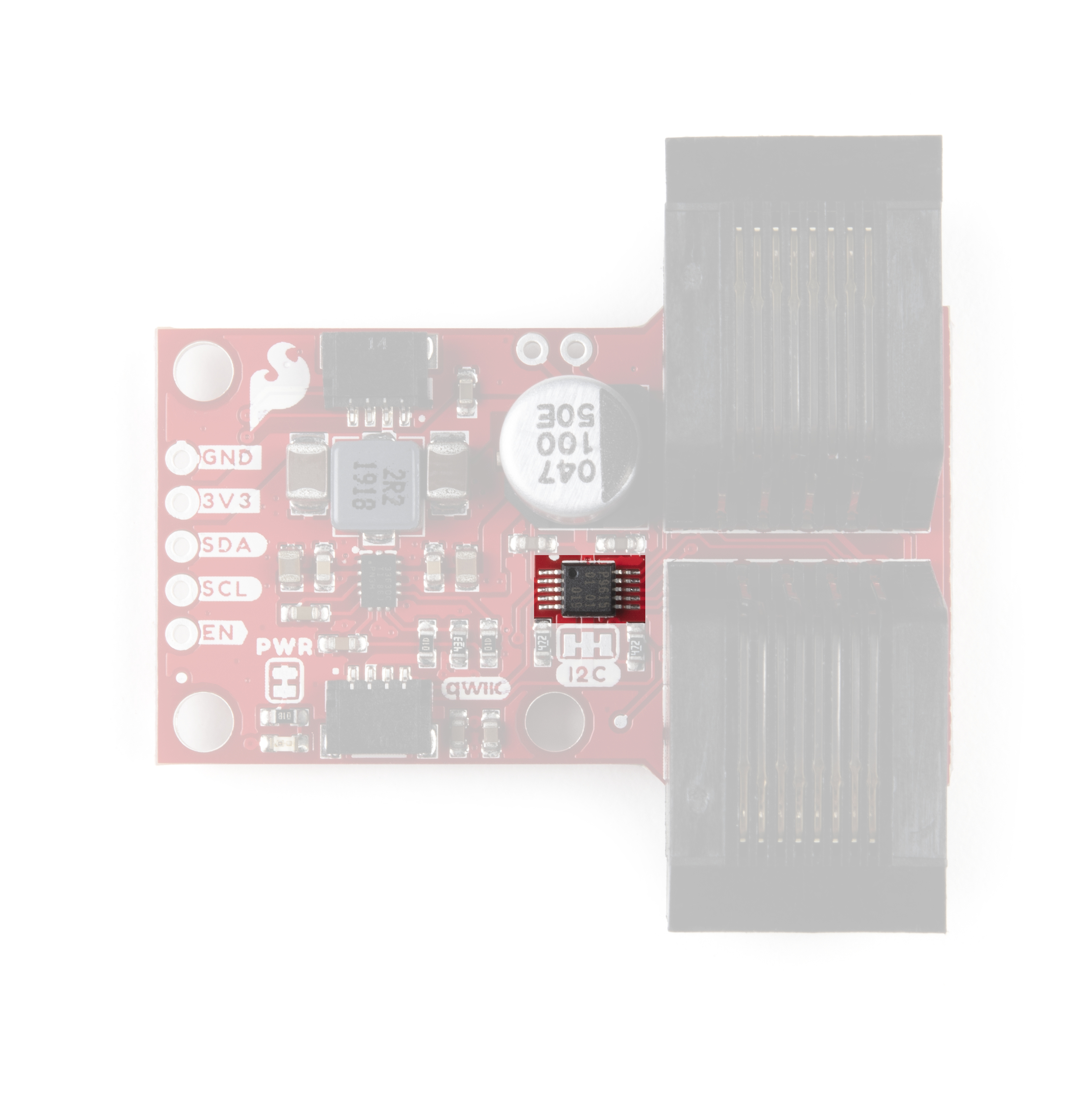
PCA9615 Bus Buffer IC
Let's take a quick look at the PCA9615 IC at the heart of the MidPoint and EndPoint. The PCA9615 acts as a bridge that translates a standard two-wire I2C bus to a four-wire differential I2C bus. Translating to a differential bus helps prevent signal disruption in noisy environments as well as extending the signal over long-distance transmissions. For detailed information about the full functionality and feature set of the PCA9615 review the datasheet.
 |
 |
The PCA9615 has two supply voltage rails: VDDA and VDDB. VDDA acts primarily as the I2C-bus side power supply and VDDB primarily is used for the differential side power supply. While the two power supplies have slightly different operating ranges (VDDA supply voltage range: 2.3-5.5V. VDDB supply voltage range: 3.0-5.5V), both the EndPoint and MidPoint default to net both voltages together at 3.3V.
The PCA9615 supports I2C clock speeds up to 1MHz though the maximum cable length is inversely related to the clock speed. At max speed, the max rated cable length is listed at 3m but can be increased at lower clock speeds. For example, in our testing of the QwiicBus with over 200 feet of Ethernet cable we observed no significant signal loss while running at the standard clock speed for the Arduino Wire Library (100KHz).
We've designed the QwiicBus MidPoint and EndPoint to have multiple configuration options for powering your QwiicBus so there is a bit to take note of before powering everything up. We cover the different power configurations further down in the Solder Jumpers sub section as well as in the Hardware Assembly section so read on for more information.
The QwiicBus boards also break out the Enable (EN) pin to a PTH header if you would like to control the PCA9615 manually. By default, it is pulled to VDDA via an internal resistor. Refer to section 7.3 of the PCA9615 datasheet for more information on using this pin.
Finally, the PCA9615 requires terminating resistors on both ends of the bus to function properly. The EndPoint includes these resistors but as the MidPoint's name suggests, it is intended to only act as a node (middle point) and therefore does not have terminating resistors. As a result, controllers must be connected to the EndPoint and will not work properly when connected to the MidPoint.
Qwiic and I2C Interface
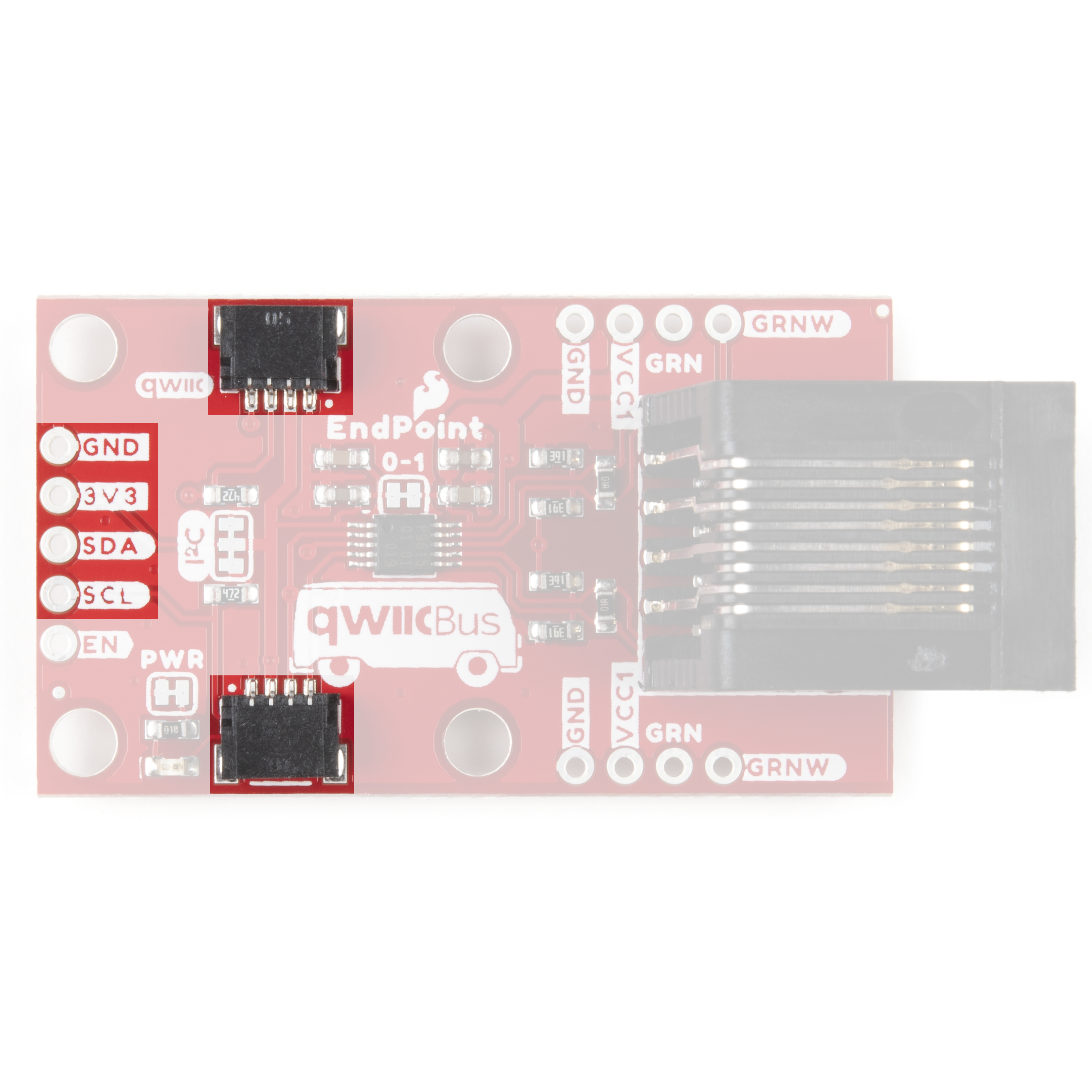
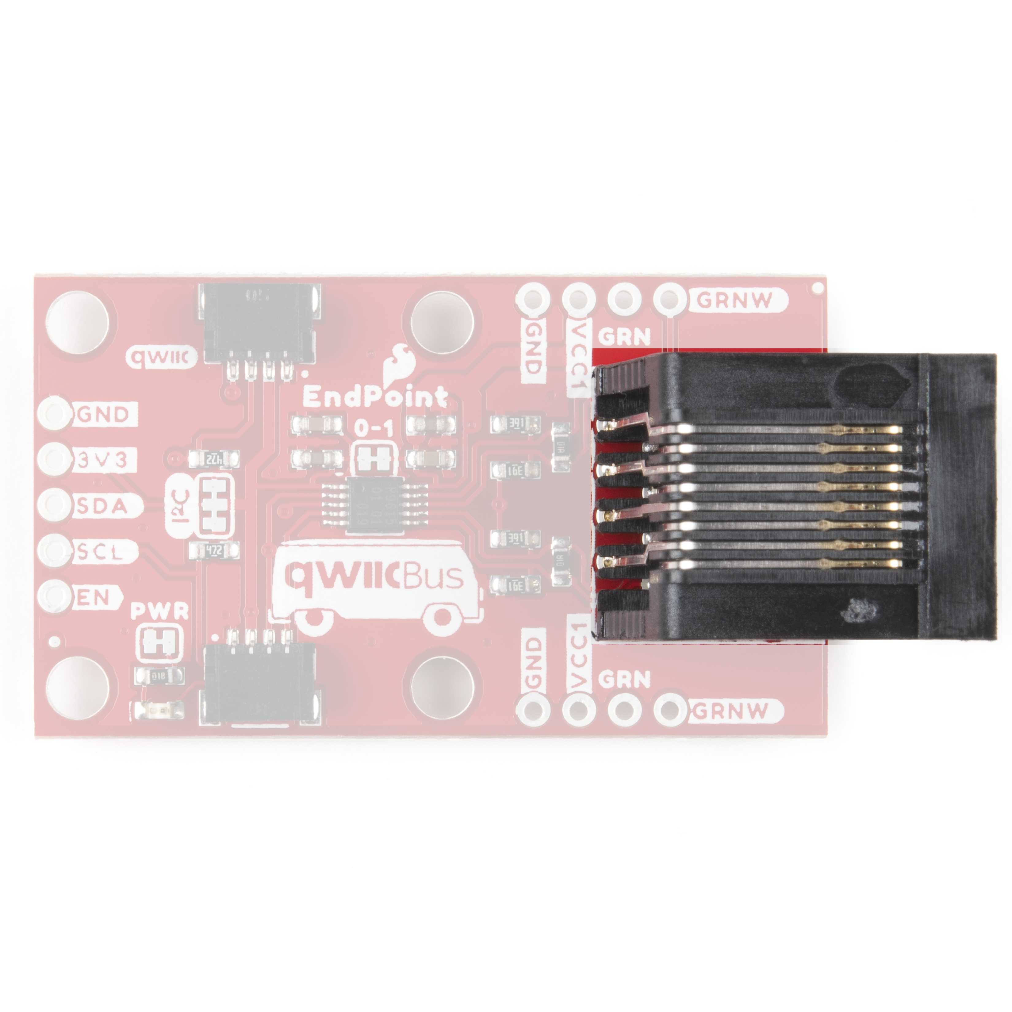
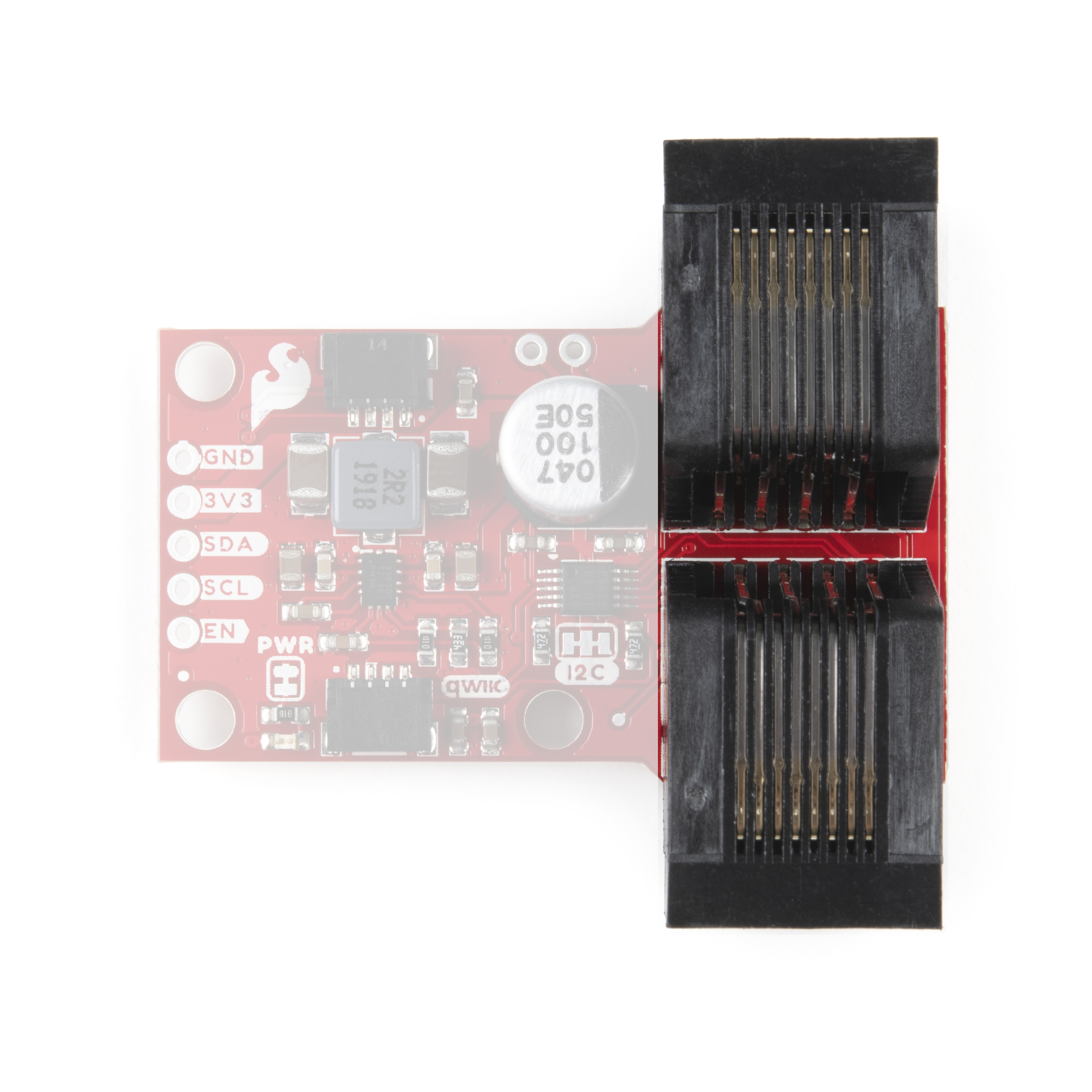
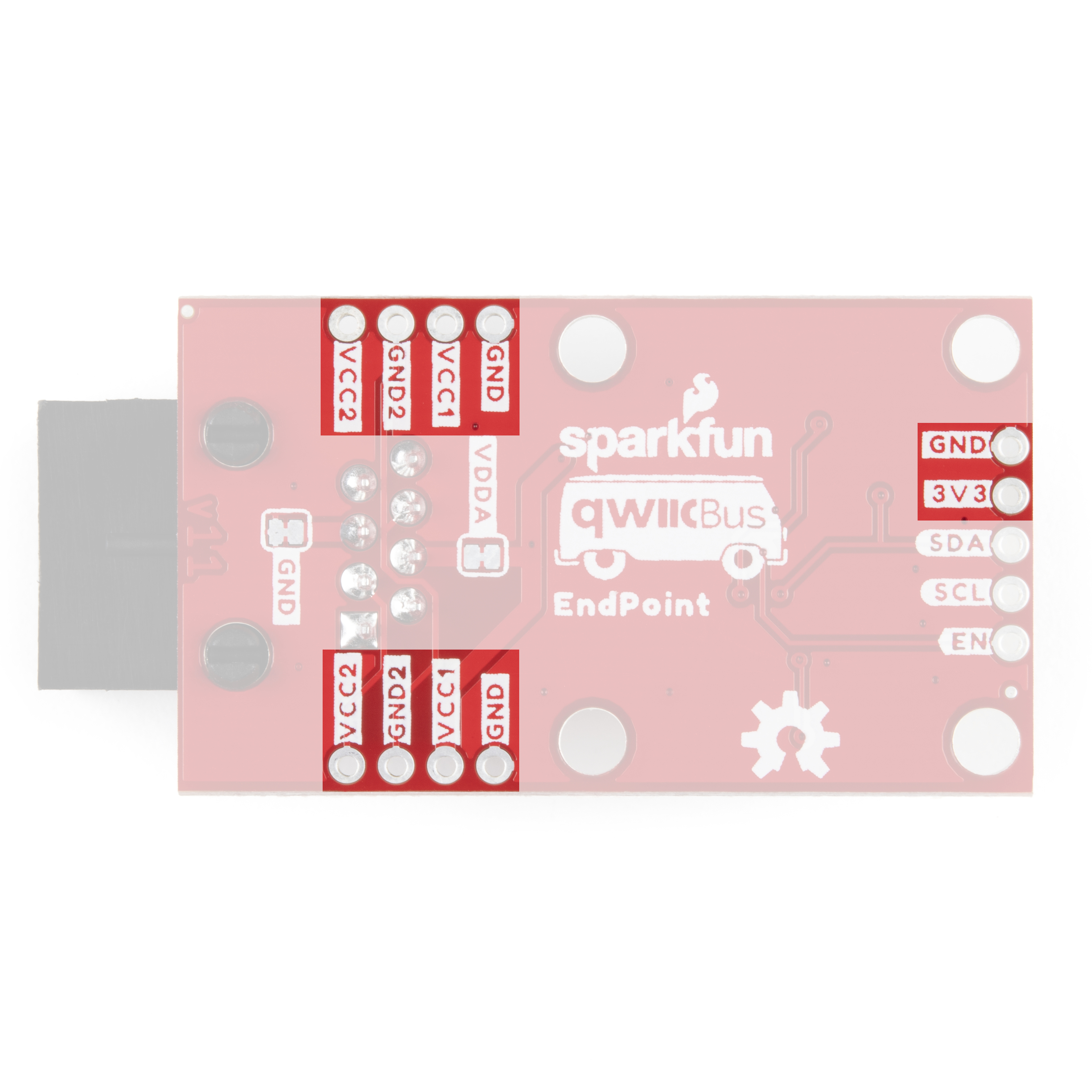
As a large portion of you readers have come to expect, the I2C pins are broken out to two Qwiic connectors so you can easily connect your QwiicBus boards to other Qwiic devices. We've also broken out the four I2C pins to standard 0.1"-spaced PTH header pins for users who prefer the standard plated through-hole connection.
 |
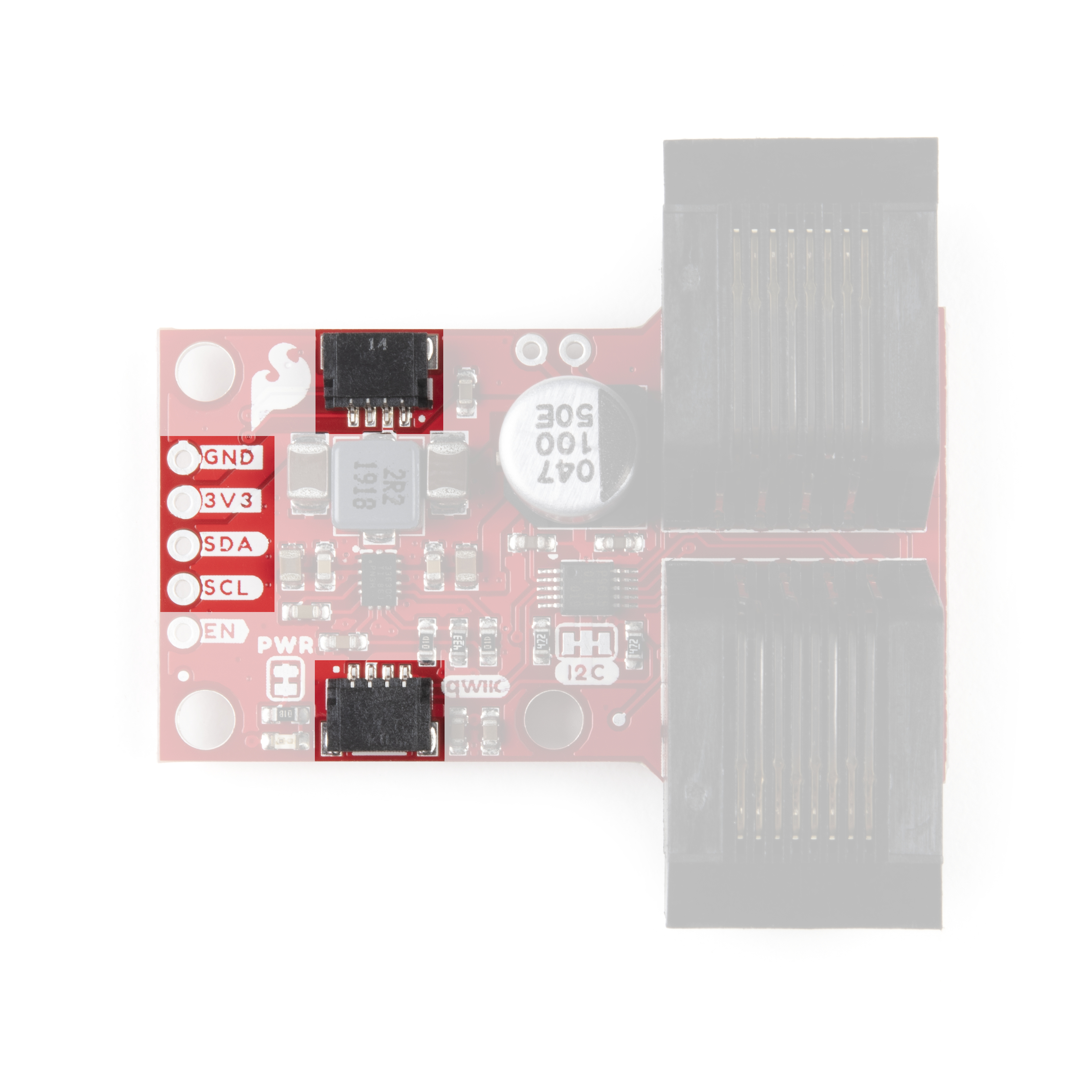 |
Differential Output and RJ-45 Connectors
The EndPoint has a single RJ-45 to send the differential signal out to another EndPoint or to your MidPoint nodes. The MidPoint comes with two RJ-45 connectors so you can easily integrate it into your existing bus.
 |
 |
Depending on your project's power needs, the unused Green and Blue twisted pairs in the Ethernet cable can be used to send 5V over the Blue pair (Ethernet pins 4 and 5) or 3.8V to 36V over the Green pair (Ethernet pins 3 and 6). On the EndPoint, the Blue pair is broken out to PTH pins labeled VCC1 and GND and the Green pair is broken out to PTH pins labeled VCC2 and GND2.
We've also broken out the VCC2 and GND2 lines to a pair of PTH pins on the MidPoint if users would like to use them for powering peripherals or running the voltage over the QwiicBus chain on separate wires.
 |
 |
VCC1 is tied to both VDDA and VDDB on the PCA9615 so long as the 0-1 jumper is CLOSED (more on that in the following sections). VCC2 and GND2 are connected to the Ethernet Green pair intended for powering the buck regulator on any attached MidPoint(s). If users are powering the QwiicBus through either of these voltage inputs, the Bypass jumper on all MidPoints must be OPENED. Using the Green or Blue pair to provide voltage to the QwiicBus requires the proper power configuration covered in the Hardware Assembly section.
Lastly, you may notice the VCC2 and GND2 PTH pins on the EndPoint are labeled GRN and GRNW when viewed from the top. The Green pair can be used as an isolated signal line in the default (System @3.3V) and Alternate 1 (VCC@5V) configurations. Note, when using the Green pair in this way, make sure the GND2 jumper(s) on any attached MidPoints are opened and the PSEL jumper on any MidPoints are either completely OPEN (Default) or set to "1".
Buck Regulator - MidPoint Only
The MidPoint includes the LMR33630 Simple Switcher® variable buck regulator from Texas Instruments®. The regulator accepts an input voltage between 3.8V to 36V so you can send higher voltages over the Ethernet cable to render any voltage drop over long cables negligable and the 3A@3.3V output provides a larger current source for any devices attached to the MidPoint. The LMR33630 has a variable voltage output that the MidPoint design sets to 3.3V.
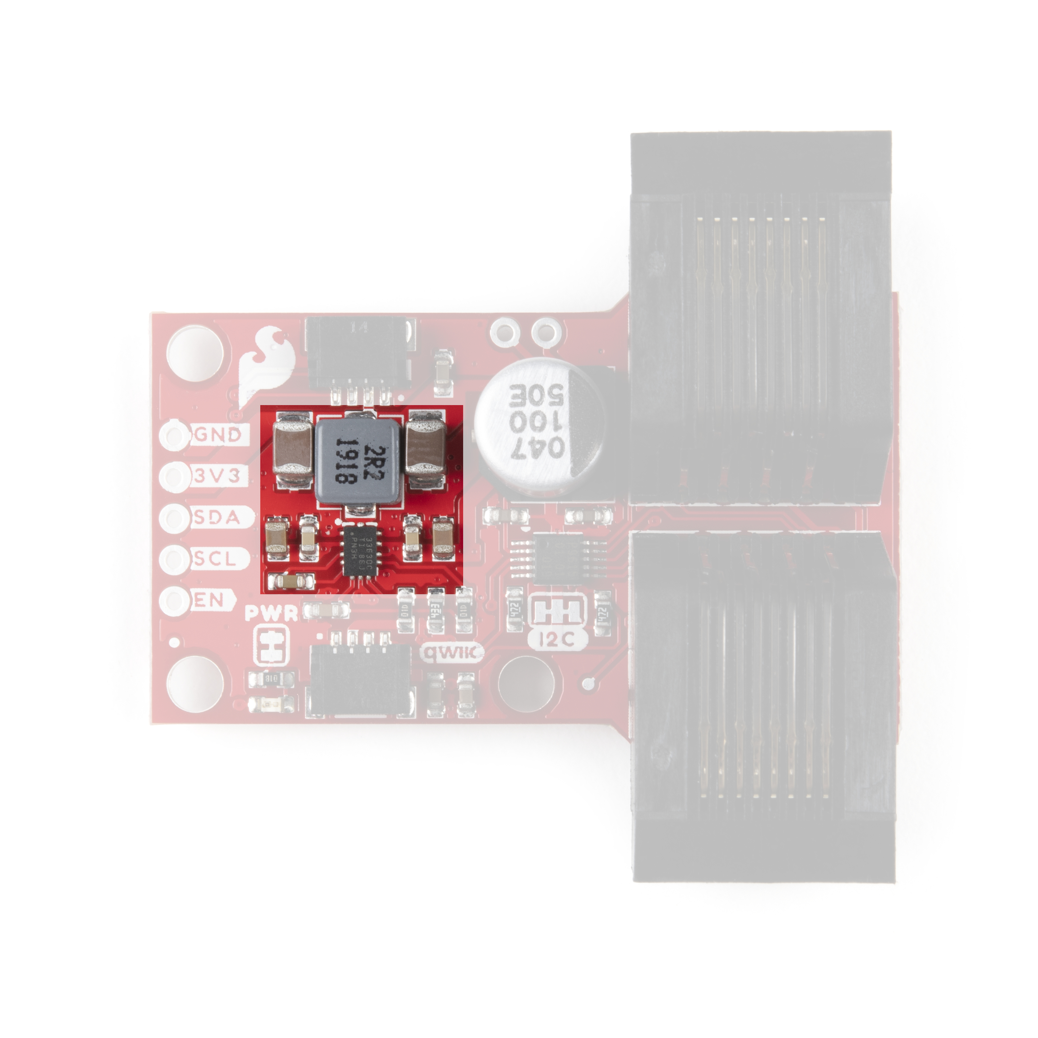
The buck regulator is not powered by default but the design features a dual jumper labeled PSEL users can adjust to enable the buck regulator to power the MidPoint(s) from a higher voltage (5V or 3.8V to 36V) via the Blue and Green pair pins broken out on the EndPoint and MidPoint. Read on to the Solder Jumpers sub-section below and the Hardware Assembly section for more information on how to use these alternate power configurations.
Solder Jumpers
In this section we'll cover the jumpers found on both QwiicBus boards and their functionality, default state and a few things to take note of prior to adjusting them.
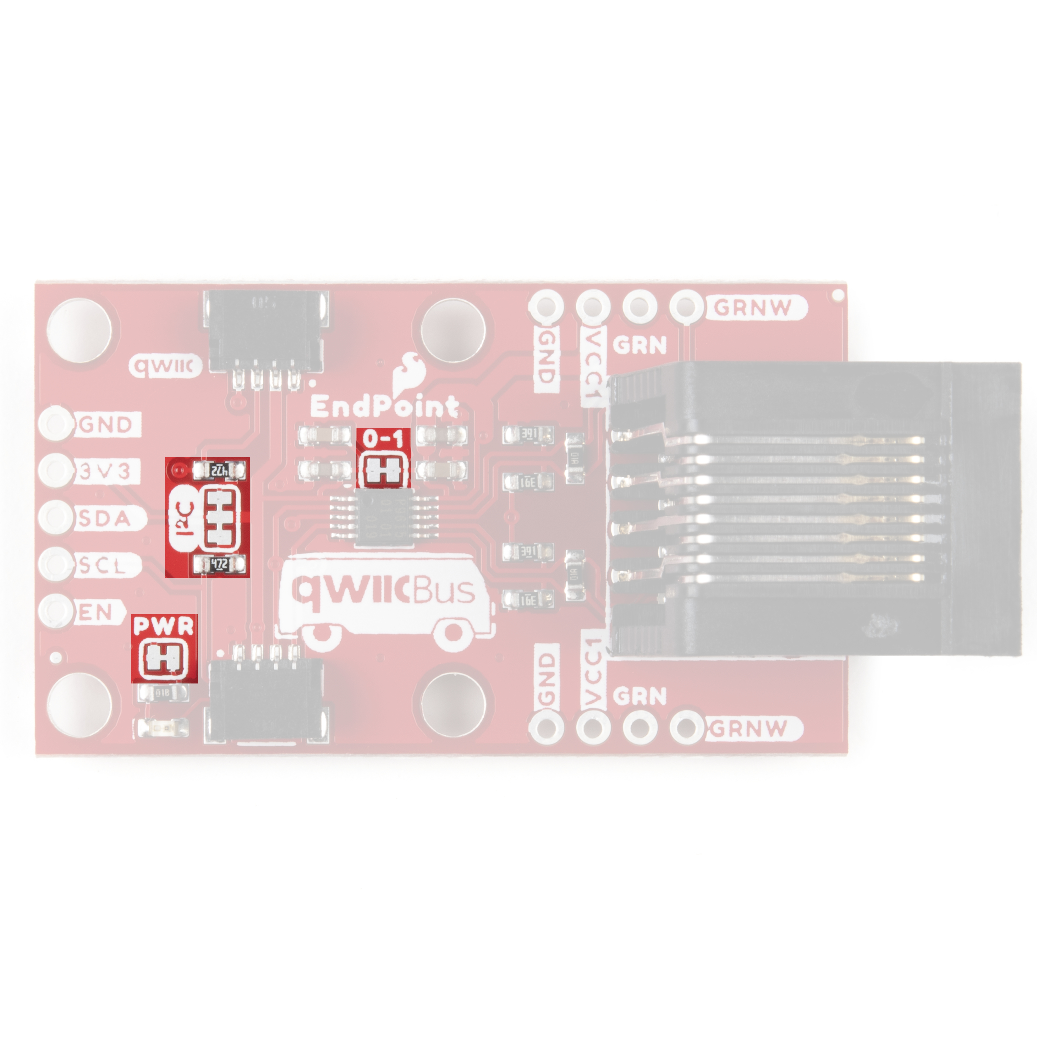
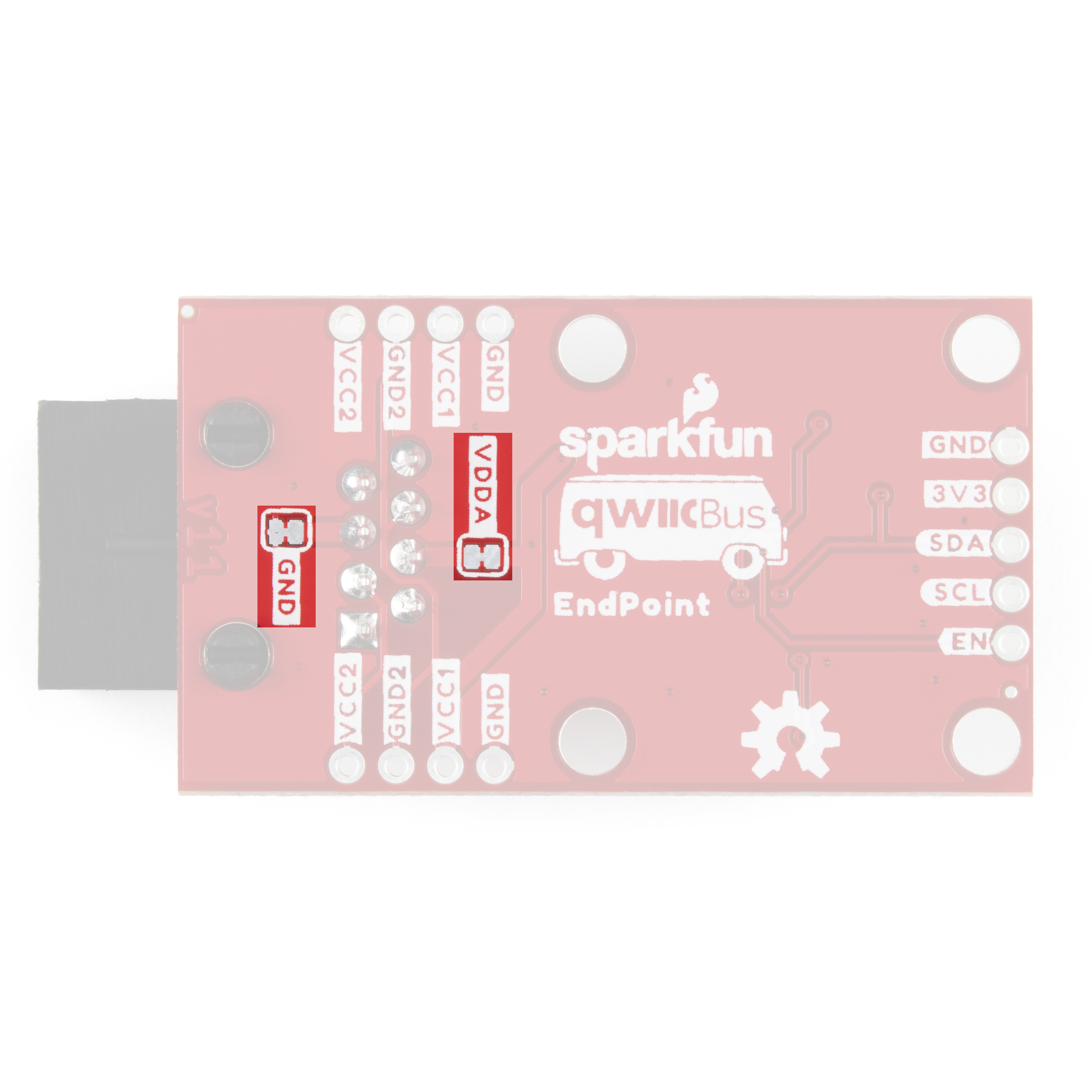
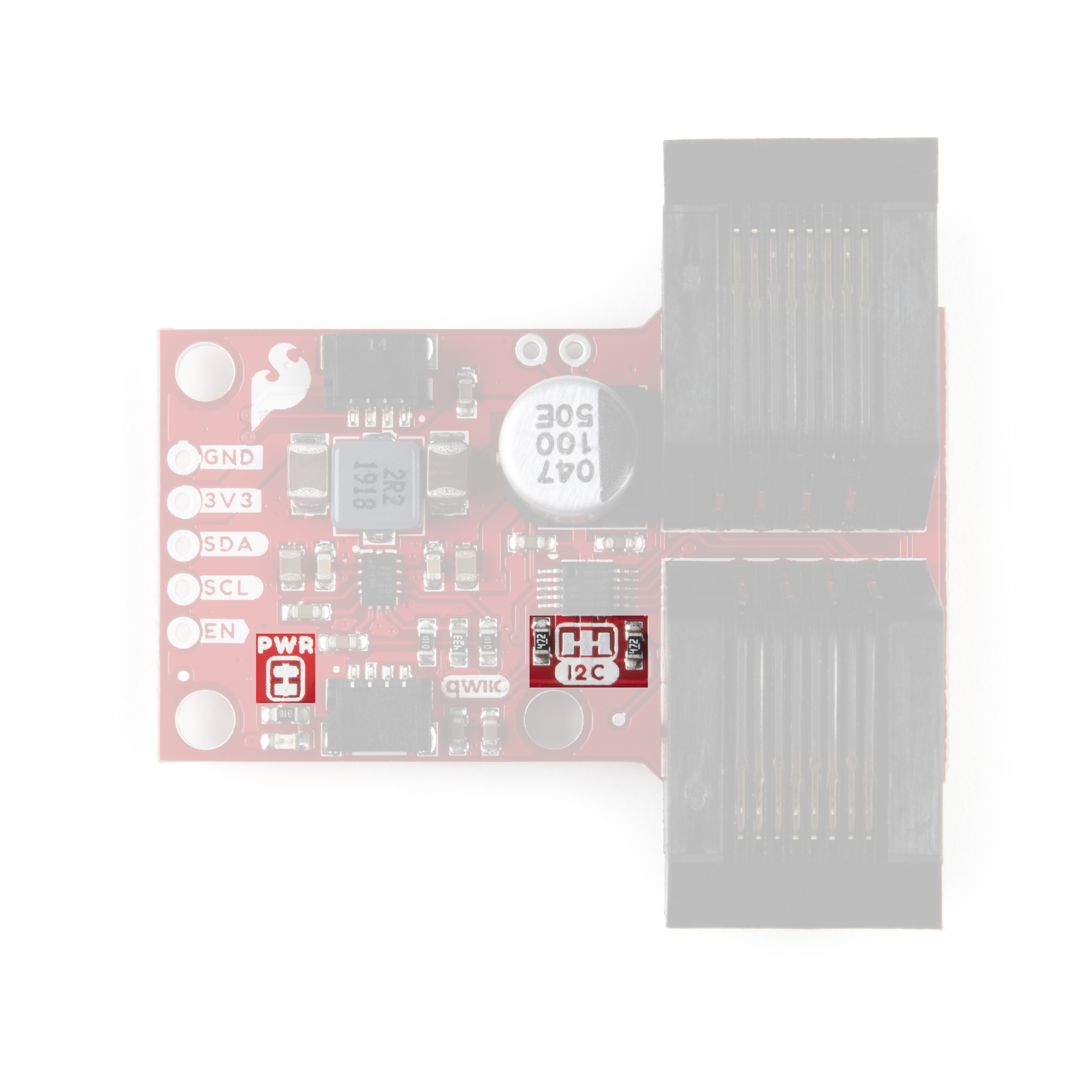
Since this guide covers both QwiicBus boards (EndPoint and MidPoint) we'll denote which jumpers are found on both boards as well as board-specific jumpers. The EndPoint's five jumpers are labeled: I2C, PWR, VDDA, GND and 0-1. The six MidPoint jumpers are labeled: I2C, PWR, BP, PSEL, GND1 and GND2.
 |
 |
| QwiicBus EndPoint Solder Jumpers - Top | QwiicBus EndPoint Solder Jumpers - Bottom |
 |
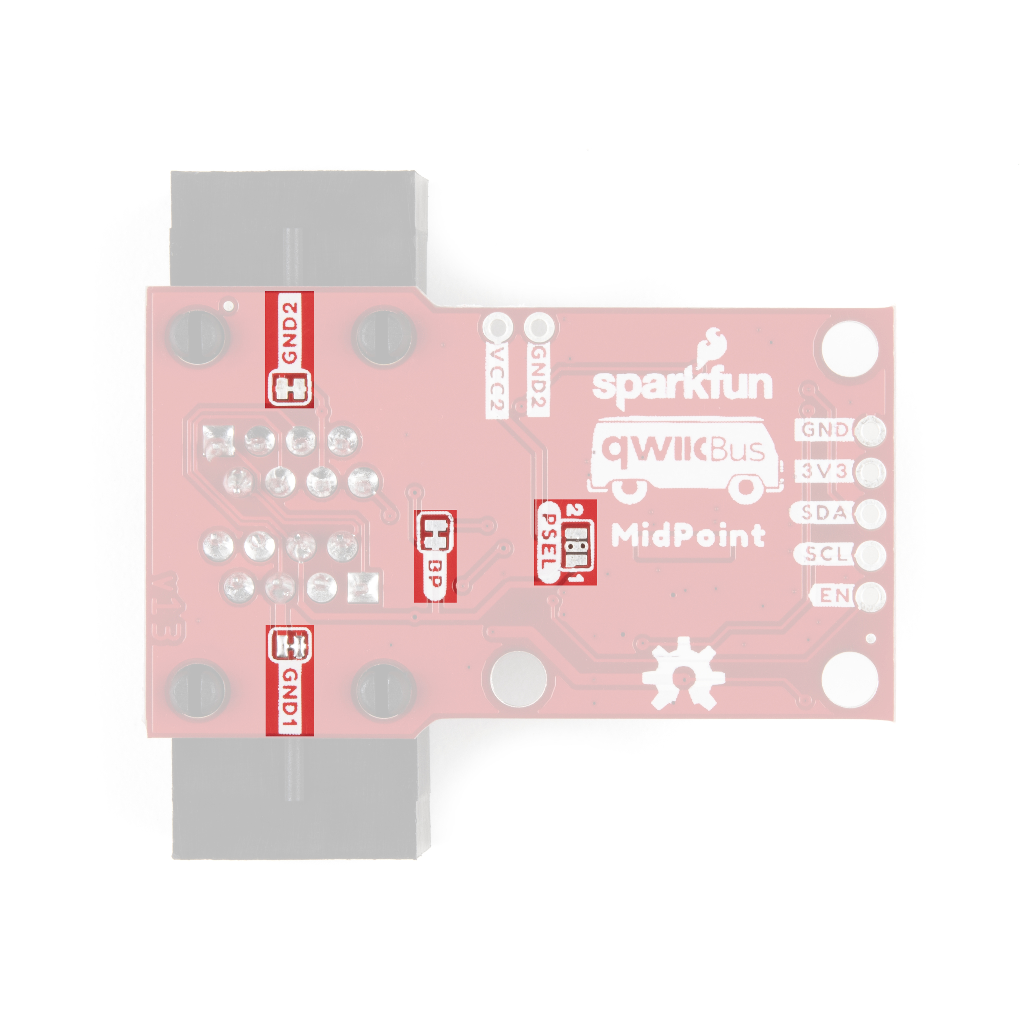 |
| QwiicBus MidPoint Solder Jumpers - Top | QwiicBus MidPoint Solder Jumpers - Bottom |
I2C Pull-Up Jumper - EndPoint and MidPoint
This jumper connects the SDA and SCL lines to VDDA of the PCA9615 (normally 3.3V) via a pair of 4.7kΩ resistors. The jumper's default state is CLOSED. To disable the pull-up resistors open the jumper by severing the trace between the three pads.
Power (PWR) LED Jumper - EndPoint and MidPoint
This jumper connects the Power LED's cathode to 3.3V via a 1kΩ resistor. The jumper is CLOSED by default. Open the jumper by severing the trace between the two pads to disable the power LED on either QwiicBus board.
VDDA and GND Jumpers - EndPoint
The VDDA and GND jumpers connect VDDA (if the 0-1 jumper is closed) and Ground to the Blue twisted pair on the RJ-45 jacks and Ethernet cable. Their default state is CLOSED. If users do not need the Blue pair for a power input, these jumpers can be opened so that pair is avaiable for other data lines or redundant power connections. Most users will want to leave these jumpers alone. If using the Blue pair as an independent signal, make sure the GND2 jumper on any MidPoints is OPEN.
0-1 Jumper - EndPoint
The 0-1 jumper nets VDDA and VDDB on the PCA9615 together. By default this jumper is CLOSED to power both VDDA and VDDB with the same supply voltage (3.3V in the default power configuration). Open this jumper if using two separate voltages for VDDA (VCC) and VDDB (VCC1). If using separate voltages, make sure they fall within the voltage ranges for VDDA (2.3V-5.5V) and VDDB (3.0V-5.5V).
Bypass (BP) Jumper - MidPoint
The Bypass jumper (labeled BP on the board) nets VCC1 with the 3.3V rail on the MidPoint. By default, this jumper is CLOSED. When the QwiicBus system is powered at 3.3V, this jumper can remain closed but if the PSEL jumper is adjusted to use anything over 3.3V to power the QwiicBus, this jumper must be OPEN.
Power Select (PSEL) Jumper - MidPoint
This dual jumper selects which voltage supplies the input voltage for the MidPoint buck regulator. The Power Select jumper defaults to all open and the buck regulator is unpowered. In this default setting, power for each EndPoint is 3.3V and provided over the Blue pair of the Ethernet cable from the microcontroller/SBC or dedicated 3.3V power supply.
If using the 5V power configuration, this jumper should be closed to set it to the "1" side. When set to "1", the input voltage is still provided over the Blue pair of the Ethernet cable but at 5V.
If using the 3.8V-36V power configuration, close the jumper to set it to the "2" side. When set to "2", input voltage is provided over the Green pair of the Ethernet cable.
GND1 and GND2 Jumpers - MidPoint
The GND1 and GND2 jumpers net both input voltages to a common ground. Both jumpers are CLOSED by default. In advanced-use cases, users can open one or both of these jumpers to reduce noise and/or prevent ground loops on QwiicBus boards further down the chain. Most users will want to leave these jumpers alone.
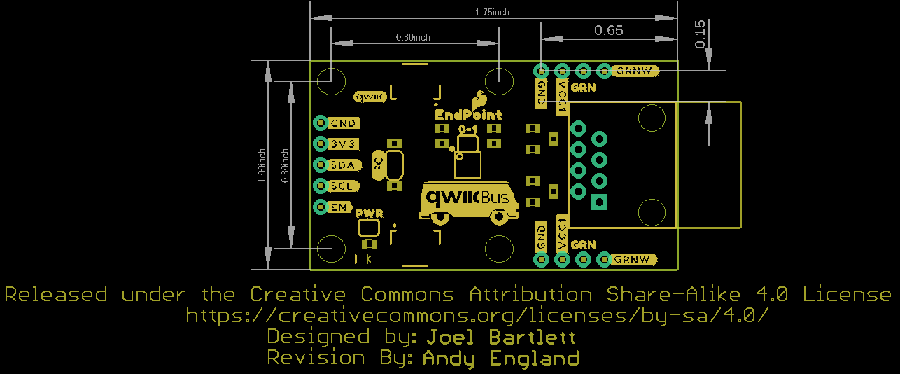
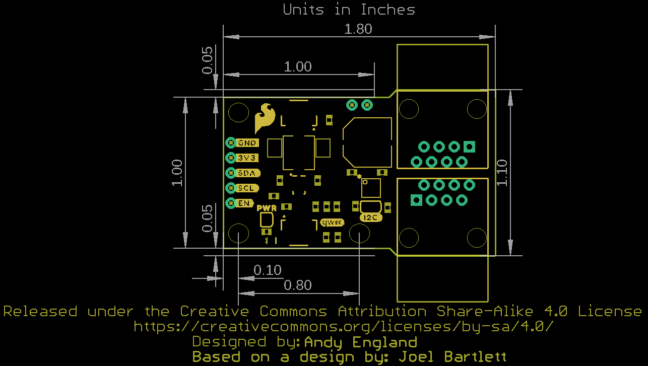
Board Dimensions
The QwiicBus EndPoint PCB measures identically to the Differential I2C Breakout at 1.75in x 1.00in (44.45mm x 25.40mm). The MidPoint measures 1.80in x 1in (45.72mm x 25.40mm) and is flared to 1.10in (27.94mm) wide at the RJ-45 end. The RJ-45 connectors extend roughly 0.30in (7.62mm)from the edge of the PCB on both boards.