Transistors
 jimblom
Symbols, Pins, and Construction
Transistors are fundamentally three-terminal devices. On a bi-polar junction transistor (BJT), those pins are labeled collector (C), base (B), and emitter (E). The circuit symbols for both the NPN and PNP BJT are below:
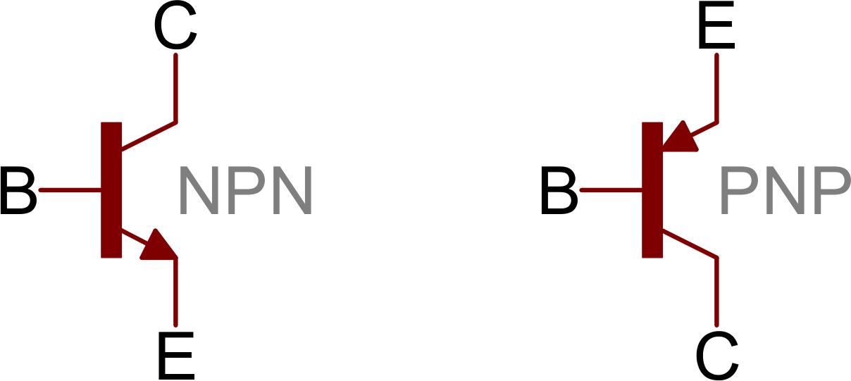
The only difference between an NPN and PNP is the direction of the arrow on the emitter. The arrow on an NPN points out, and on the PNP it points in. A useful mnemonic for remembering which is which is:
NPN: Not Pointing iN
Backwards logic, but it works!
Transistor Construction
Transistors rely on semiconductors to work their magic. A semiconductor is a material that's not quite a pure conductor (like copper wire) but also not an insulator (like air). The conductivity of a semiconductor -- how easily it allows electrons to flow -- depends on variables like temperature or the presence of more or less electrons. Let's look briefly under the hood of a transistor. Don't worry, we won't dig too deeply into quantum physics.
A Transistor as Two Diodes
Transistors are kind of like an extension of another semiconductor component: diodes. In a way transistors are just two diodes with their cathodes (or anodes) tied together:
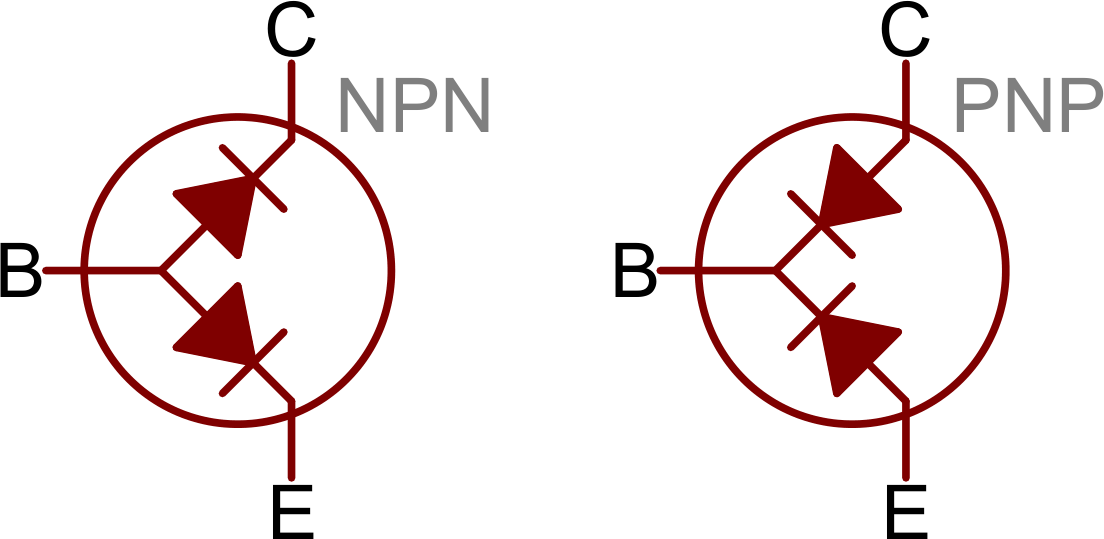
The diode connecting base to emitter is the important one here; it matches the direction of the arrow on the schematic symbol, and shows you which way current is intended to flow through the transistor.
The diode representation is a good place to start, but it's far from accurate. Don't base your understanding of a transistor's operation on that model (and definitely don't try to replicate it on a breadboard, it won't work). There's a whole lot of weird quantum physics level stuff controlling the interactions between the three terminals.
(This model is useful if you need to test a transistor. Using the diode (or resistance) test function on a multimeter, you can measure across the BE and BC terminals to check for the presence of those "diodes".)
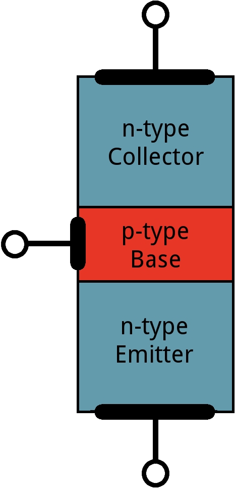
Transistor Structure and Operation
Transistors are built by stacking three different layers of semiconductor material together. Some of those layers have extra electrons added to them (a process called "doping"), and others have electrons removed (doped with "holes" -- the absence of electrons). A semiconductor material with extra electrons is called an n-type (n for negative because electrons have a negative charge) and a material with electrons removed is called a p-type (for positive). Transistors are created by either stacking an n on top of a p on top of an n, or p over n over p.
With some hand waving, we can say electrons can easily flow from n regions to p regions, as long as they have a little force (voltage) to push them. But flowing from a p region to an n region is really hard (requires a lot of voltage). But the special thing about a transistor -- the part that makes our two-diode model obsolete -- is the fact that electrons can easily flow from the p-type base to the n-type collector as long as the base-emitter junction is forward biased (meaning the base is at a higher voltage than the emitter).
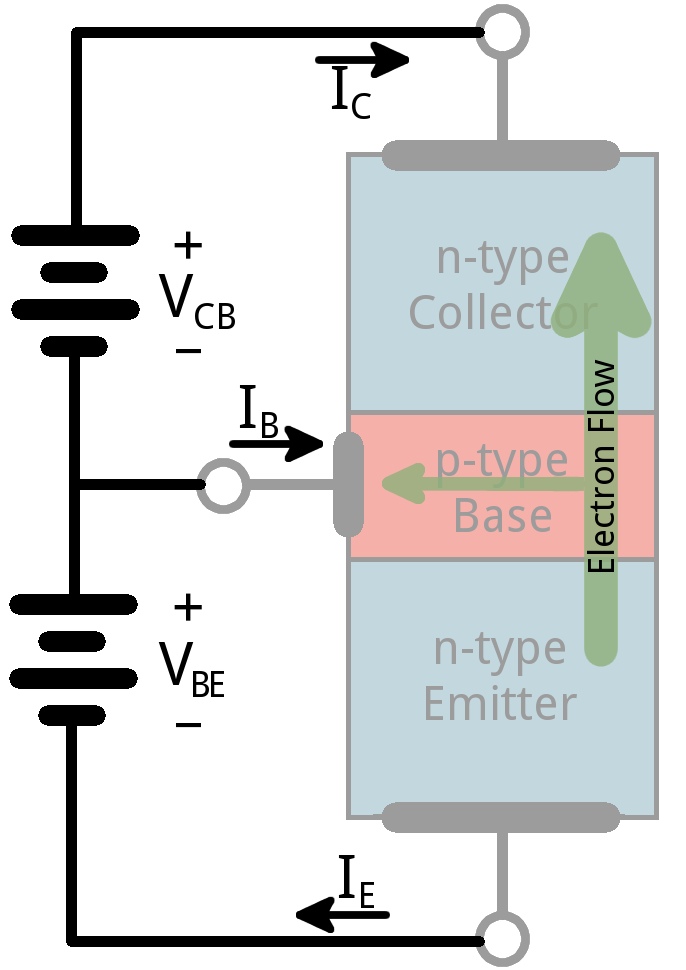
The NPN transistor is designed to pass electrons from the emitter to the collector (so conventional current flows from collector to emitter). The emitter "emits" electrons into the base, which controls the number of electrons the emitter emits. Most of the electrons emitted are "collected" by the collector, which sends them along to the next part of the circuit.
A PNP works in a same but opposite fashion. The base still controls current flow, but that current flows in the opposite direction -- from emitter to collector. Instead of electrons, the emitter emits "holes" (a conceptual absence of electrons) which are collected by the collector.
The transistor is kind of like an electron valve. The base pin is like a handle you might adjust to allow more or less electrons to flow from emitter to collector. Let's investigate this analogy further...