Using EAGLE: Board Layout
 jimblom
Previously on Using EAGLE
EAGLE's board designer is where a good portion of the magic happens. It's here where the dimensions of the board come together, parts are arranged, and connected by copper traces. In the board editor, the conceptual, idealized schematic you've designed becomes a precisely dimensioned and routed PCB.
In this tutorial we'll cover every step in EAGLE PCB design: from placing parts, to routing them, to generating gerber files to send to a fab house. We'll also go over the basics of EAGLE's board editor, beginning with explaining how the layers in EAGLE match up to the layers of a PCB.
Create a Board From Schematic
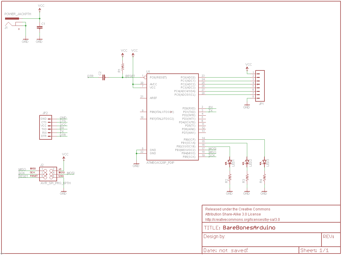
Before starting this tutorial, read through and follow along with the Using EAGLE: Schematic tutorial (not to mention the Setting Up EAGLE tutorial before that). The schematic designed in that tutorial will be used as the foundation for the PCB designed here.
To switch from the schematic editor to the related board, simply click the Generate/Switch to Board command --  (on the top toolbar, or under the File menu) -- which should prompt a new, board editor window to open. All of the parts you added from the schematic should be there, stacked on top of eachother, ready to be placed and routed.
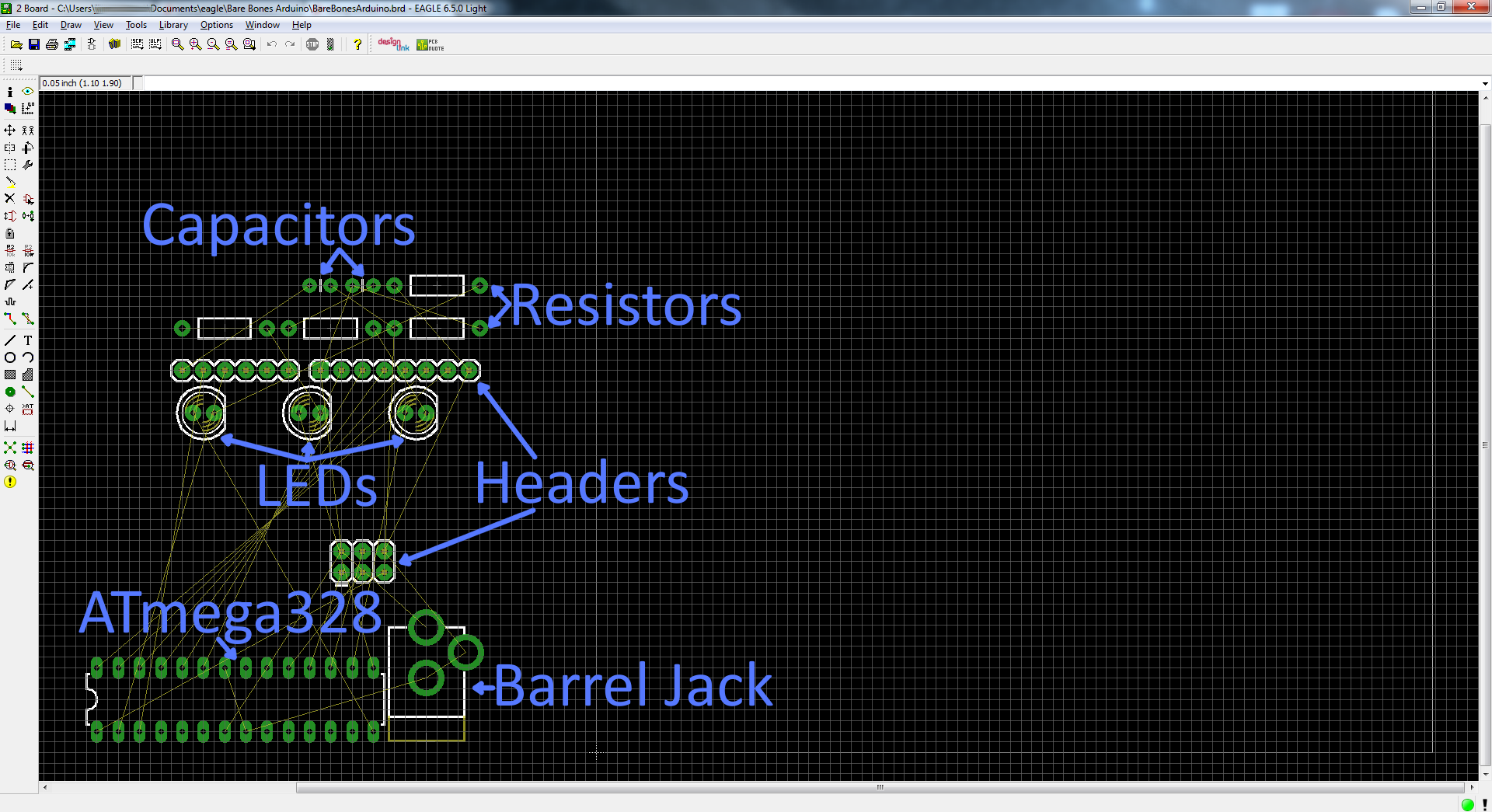
The board and schematic editors share a few similarities, but, for the most part, they're completely different animals. On the next page, we'll look at the colored layers of the board editor, and see how they compare to the actual layers of a PCB.