Enginursday: Innovative Testbed Design (Part 1 of 2)
Join us as we give some insight into the progress made in SparkFun’s testbed design over the past eleven years, and an in-depth look at our most recent production testing tool, the Flying Jalapeno.

Note, if you like to jump to part 2 of this blog, click here:
It’s fun to be on the quality control side of things. Not only do we get to play with all the new widgets ahead of release, we are constantly faced with new challenges and pushed to innovate testbed design. Sometimes new products require new features on a testbed, and that pushes us to innovate. Sometimes we discover a reliability issue in production, and that pushes us to revise hardware to make something more robust. We've progressed a lot over the years. Let's look back and highlight some of the innovations that allow us to design, build and code new testbeds really quickly.
Back in the day
We used to have some fairly finicky test fixtures back in the day. As a production tech in 2007, I remember very carefully handling the fixtures to make sure I didn't break any of the many, many green wires (and I was lucky if it worked 50 percent of the time).
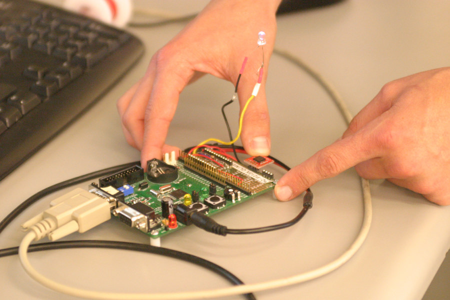
Test fixture from 2008 using bare male headers to connect to the product...eeek!
As you can see above, this early testbed uses male headers facing up to make a temporary connection to the product. The technician would have to slide the headers into the products PTH headers on the side of the product, and then apply pressure to either side to attempt to make a connection during testing. It took a very steady hand to get this sucker to work every time. If you'd like to check out more info about our older test fixtures and general quality control progress, check out these tutorials:
- Sneaky Footprints (2008)
- PogoBeds: SparkFun Production and Testing (2009)
- Ganged Programming with AVR ISP MKIIs (2011)
- Constant Innovation in Quality Control (2013)
- Enginursday: A new and improved IOIO-OTG! (2016)
- Raspberry Pi Stand-Alone Programmer (2018)
Custom layouts
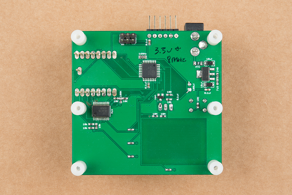
Testbed made with custom PCB layout using mostly SMD commponents
In 2009 (ish), we started laying out custom PCBs for every new testbed. This was nice because it kept the designs small and self contained. Another advancement here was using pogopins to make a nice temporary connection to the product. This style of testbed design actually proved to be the "norm" for quite a while. At the time, and still to this day, we build all of our test fixtures by hand with an iron (even all the SMD parts). We just couldn't justify ordering a stencil when we could get by with an iron and a steady hand. Even if it did have some more difficult parts that require hot air to place, we wanted to keep our rework chops up to snuff!
Modular Designs
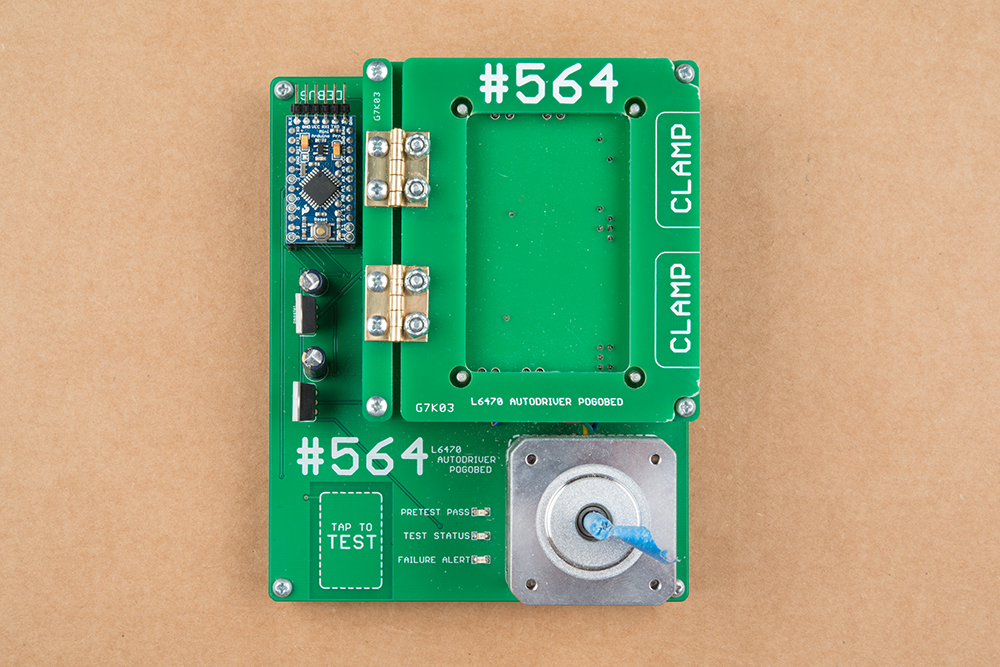
Testbed designed around an Arduino Pro Mini and a custom base layer PCB
Here we have a stepper motor driver testbed. This is a good example of how we were able to use an Arduino Pro Mini as the main "brain" of the testbed, and then add the additional components needed to a custom PCB layout. This approach to testbed design became known as the "modular" approach, and cut down on the SMD work needed to assemble a testbed. It was also nice to know that production had tested the Pro Mini on your testbed, cutting down on any troubleshooting when you first power up.
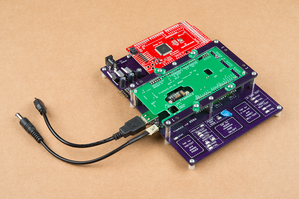
Testbed using a Arduino Mega Pro and a custom base layer PCB
Here is a second example of a "modular" designed testbed, except this time we needed more GPIOs. This required using a Arduino Mega Pro instead of the Pro Mini. This again helps cut down on assembly time, although soldering up all of the PTH headers on the Mega Pro Board, and its mating female headers on the testbed, still does take some time. You may notice that this has quite a mix of color in the PCBs. I seem to remember having to rush order this from OSH Park in order to keep up with the Free SoC2 product launch schedule. Thanks OSH Park!!
Stand-alone programming
It had always been a dream of ours to move testing and programming away from using the production techs' Windows computers. This is because each time Windows would auto-update, we would be bombarded with driver issues. We ended up going with a Raspberry Pi-based solution and designing our own custom HAT, the SparkFun Pi AVR Programmer HAT. Read all about it in the following tutorial:
Pi AVR Programmer HAT Hookup Guide
July 26, 2018
In this tutorial, we will use a Raspberry Pi 3 and the Pi AVR Programmer HAT to program an ATMega328P target. We are going to first program the Arduino bootloader over SPI, and then upload an Arduino sketch over a USB serial COM port.
Custom Generic Hardware
As we designed more and more testbeds, we found that they needed similar things. This is why it made sense to make a single design that included most of the features we needed, and then make custom “daughter” boards that are specific to each product.
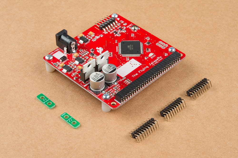
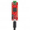
The Flying Jalapeno testing tool in all its glory!
Above, is our in-house designed Flying Jalapeno. We use this on most new test fixtures, and it dramatically decreases testbed design and assembly time. Stay tuned for a more in-depth look at the hardware design of this tool, and the accompanying Arduino code library.
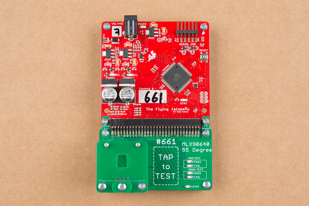
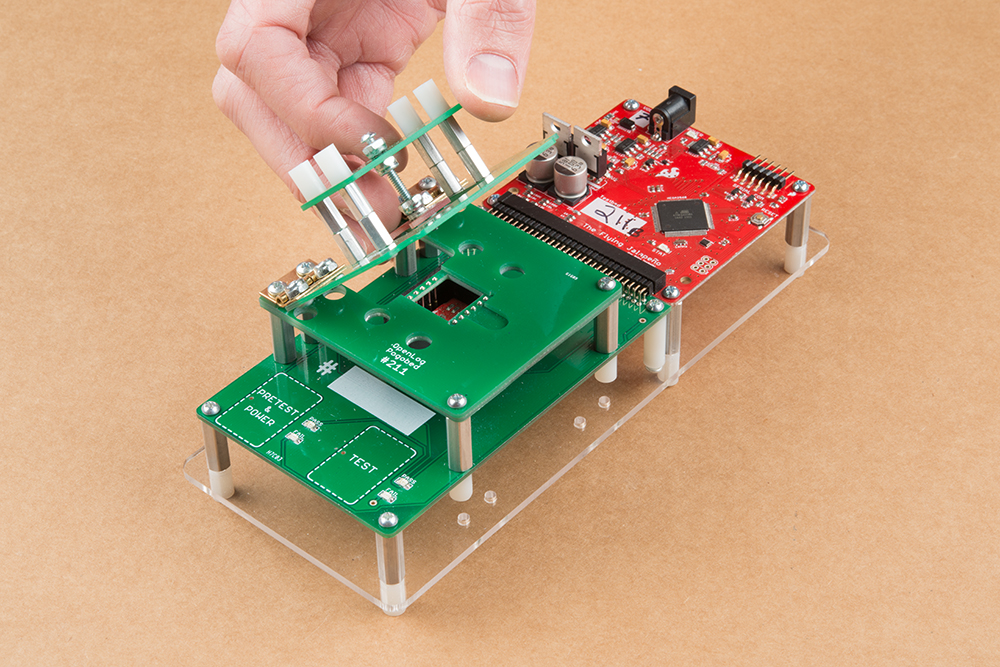
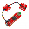
Testbed for an IR Array sensor using the Flying Jalapeno
As you can see above, this testbed is made up of two parts. The top section (the red PCB) is the Flying Jalapeno, and the bottom section (the green PCB) is the custom daughter board for the product. This particular testbed is designed to test the SparkFun IR Array Breakout. Because we receive the Flying Jalapeno assembled (and tested) from production, the assembly time for this test fixture is reduced to simply building up the smaller bottom section. That's just a 2x30 header, five LEDs and four pogopins. Piece of cake!
Laser-cut Acrylic parts
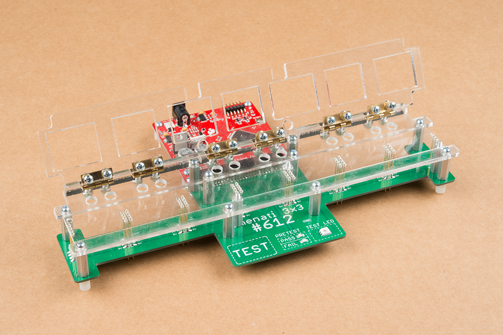
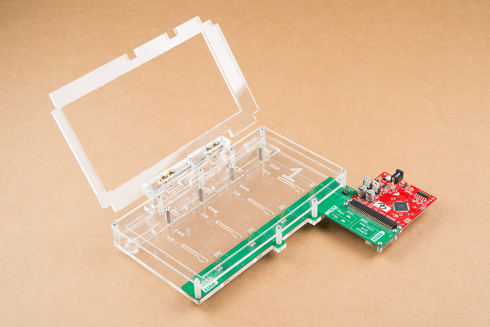
Testbed using the Flying Jalapeno and lazer-cut acrylic parts
Here is a fairly recent testbed design for testing the Lumenati 3x3. Occasionally, we will cut certain layers on our laser cutter using clear acrylic. Not only does this look slick, but it saves us money, because previously we would have been ordering those layers from a PCB fab house and that can get pretty costly for large testbeds. Also, this allows us to fine tune the laser-cut layers in house. We can tweak the design as necessary and have a new part cut in just minutes!
A few more beauties
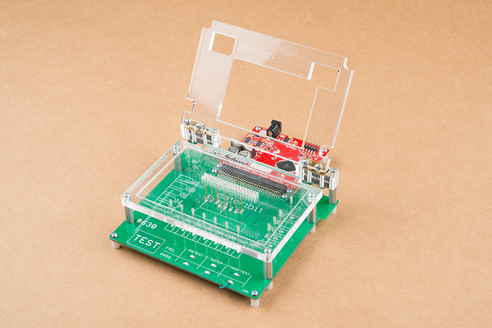
GatorBit testbed
OpenLog testbed with unique "waffle top"
RedBoard Edge testbed
Stay tuned for Part 2
Join us ~~next week~~ in a couple weeks as we give a more in-depth look at all of the hardware choices inside the Flying Jalapeno, and dive into the accompanying Arduino code library. For a sneak peak, take a close look at the following picture, and see if you can spot any design flaws. There are actually a few things that we plan to change on a future revision to this design, but I challenge you to find as many as you can. The first commenter to spot the flaw I am thinking of will get extreme street cred and I will personally mail you a Flying Jalapeno!
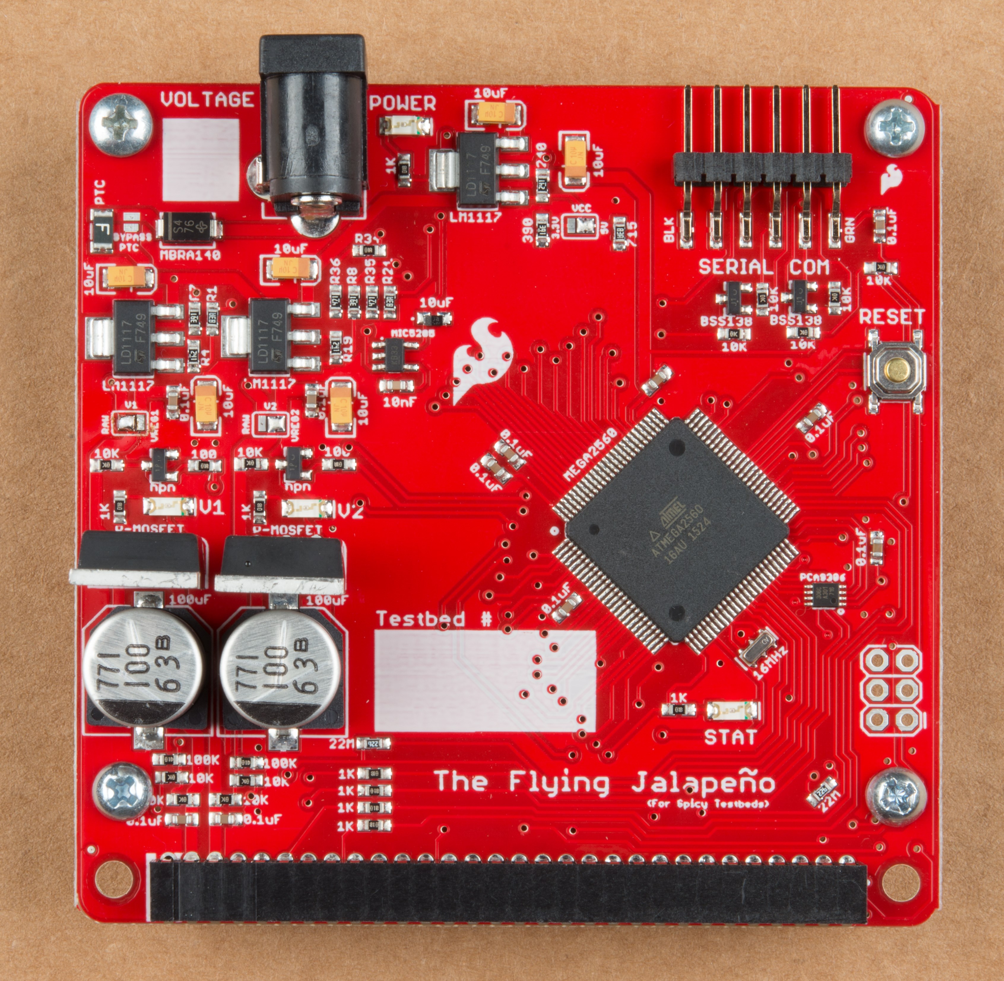
Detailed pic of the Flying Jalapeno
Also, if you have any testbed design stories to share (I’m looking at you, #773), or any questions about SparkFun testbeds, please feel free to post a comment below. Thanks for reading and we'll see ya ~~next week~~ in a couple weeks!
Note, if you like to jump to part 2 of this blog, click here:
More Testbed Images from dksmall
Thanks again everyone for all the conversation and feedback below! Dksmall has chimed in a couple times and even had some images to share. Please check them out as this final addition to the blog. Also, we will be working with Dksmall to write a guest blog post, highlighting some of their testbed development and experiecne in the field over the past 35 years!

|

|

|

|

|

|

|

|

|


Love the name!
Sincerely, Team Flying Jalapeno (AVC Has-beens)
Hey Tone! I was hoping you'd find this post! You definitely deserve all the credit for an awesome name. It was kind of random, but I remember thinking, "Why not name this after my favorite AVC teamname?" I have always been stoked on the team names at AVC, but yours really stuck out for me, cause of my slight obsession with flying RC planes (and good salsa). But I do remember seriously considering "Daisy Rover" and "Lawn Dart". Can you remember any other good ones?
When I tell people about the history of this name, it always brings a smile to learn about a team of engineers designing an autonomous flying robot named the Flying Jalapeno. And your logo was so great and hilarious. And I also love people throwing it around with a straight face when we are talking "serious business" about the code library or any future testbed designs. Sadly, it has also been commonly referred to as just "FJ". Doesn't have the same effect :)
Also, I thought you might enjoy knowing that your name has inspired future testing tool names as well. One of our test developers is currently working on the Flying Serrano (a smaller 328 based version).
Pete! So sorry I just now saw this.... and it totally made my day. I passed the word along to the other guys, everyone is excited that we had a chance to bring some joy to the SF team. I think I had sent some logo stickers to Nate or someone a few years back after the band wrote the "Spicy Sky" song, so we had a feeling you were partial. :)
Keep up the great work!
Just noticed that the serial header is SMD. I'd be inclined to make it PTH, as this is something that can be susceptible to some stress, and therefore could be prone to breaking off if SMD.
Hey 773, Another good point, for sure. I usually like to keep the serial debug header PTH, and actually opt to use PTH connectors on most testbeds. But with this design, I opted to decrease the time spent at the Selective Solder Machine. Production was already gonna have to SS the big 2x30, the Mosfets and the Barrel Jack. (which by the way, I always go with PTH barrel jacks - that has been a bit of a challenge on our Redboard, because AOI has trouble seeing the very slight "pillow style" cold joints.
The good news is that we haven't seen a single SMD 1x6 header be damaged on a Flying Jalapeno yet, so everyone is being careful enough. The other thing we have going for us here, is that it is usually only inserted once during setup and then left alone for the duration of testing a single batch. I did opt to keep in positioned in the design so that the headers are not overhanging the edge of the PCB. We've had plenty of testbeds with overhang pin connectors, and they always end up getting bend during handling or placement in the bin, and sometimes even cracked off.
As always, thanks for your feedback!
Check out some new awesome testbed pictures posted above (from 1986 to 2016). Thanks for sharing dksmall! There are some real beauties in there. Dang, that is some serious wire wrapping!!
To see the images, scroll up to the end of the blog content, or follow this link to the header section. Note, you can click on each thumbnail to see a higher resolution image if you like.
Also, we will be working with dksmall to write a guest blog post, highlighting some of their testbed development and experience in the field over the past 35 years!
Enlarging the image, I finally noticed that it appears that both the TX and RX lines on the "SERIAL COM" connector are wired to the source pin of a BSS138 MOSFET.
Also, that MBRA140 is only rated for 1A, but there is a potential for much higher currents. (And, at least once populated, there's no visible indication of polarity for this diode.)
Hi Pete! Here are a few things I noticed:
Hey Steve, Thanks for checking this out! All valid points, but still not the one I'm thinking of.
Via tenting is an age old issue around here. We are always checking the eagle files and gerbers before ordering to ensure their covered. The Eagle DRC can actually open them up (even if you don't want it too), so always make sure to view the "tStop" and "bStop" layers before CAMming up your gerbers.
These vias on the Flying Jalapeno are definitely tented full in the gerbers, but our fab house, Gold Pheonix, has decided to pull back the silk a bit around drill hits. The mask is really the most important thing, and they did allow that to cover them up. But the other thing that's going on here is that, usually once you get up to 20 mil via drill hits or bigger, the mask can't actually fill the drill hit, so it looks uncovered. Sometimes, even though the mask was manufactured over the edge of the drill hit, it will still expose the edge and there is a little tiny ring of metal exposed. I probably should have just gone with 15 mil via hits, those usually look better, and have sufficient plating for any of my current needs (which is barely anything on most data IO lines).
If you look at a more recent board like the Qwiic Twist, you can see that these 12 mil vias are fully covered in mask (most of the time), and silk can print over them pretty nicely. Although, I will say, we do our best to avoid silk over vias on all storefront designs.
And good catch on the mosfets not having room for heatsinks. I definitely overlooked this, but luckily, we haven't needed them on any testbed designs so far. Most of our products require such minimal current, that these mosfets stay cool as is.
Thanks!
May be serial comm to be a through hole part for durability? I have had problems with these SMT headers being too easily knocked off.
Hey 403, Thanks for looking! Indeed PTH is always stronger and usually the way to go for test jigs. The SMD choice here was intentional to save assembly time. More details at this comment here. Thanks!
Without knowing the range of use cases, can't say for sure if it is a flaw. The thing I noticed was that you used fairly large power MOSFETs but placed them such that you can't mount a heat sink. If you flipped them 180 you could. Was also thinking they were also sticking up a bit, could be prone to getting whacked loose, that there was enough unused board space to permit laying them flat and getting a fair amount of heat sinking as bonus. However looking at a different angle shows those caps are almost as high so perhaps not as big a problem?
Hey John, Good catch, but sorry, not the one. I totally didn't even think of heat sinks while designing this, or after using it so many times. Whoops! I guess we just have pretty minimal power requirements for most of our products and so these power circuits are pretty overkill (even without heat sinks).
The only testbed that ever used heat sinks (that I can remember) was for our Stepoko motor driver. I usually share that one on Friday tours because it's enormous and has some cool acto-botics parts with swinging arms, magnets and reed switches. The entire test apparatus I think is about 10"x15" inches (a full QC testbed PCB Panel) and has some seriously beefy traces and stepper motors.
About them getting whacked loose. A valid concern. They do occasionally get bend over and touch the nearby housing of the capacitors, but I haven't seen this cause a problem or crack off yet.
I will say... the error I'm thinking of does not involve a physical weakness, unless, I guess you are thinking that the microscopic internal movement of particles inside transistors being weak in some specific instance.
Thanks!!
Strapping to connect the level shifter to V1 or V2?
Hey Madbodger, Thanks for commenting! What do you mean by strapping? I'm guessing, like a jumper option? If so, that's an interesting improvement. Currently the logic level conversion (on the serial UART lines) is matching the ATMega2560's logic level. This is not the error/feature I was thinking of... but I will say... thinking about logic level is getting warm.
Thanks!!
I'm not sure if this is the case, but it almost looks like there are a few isolated ground planes around the power supply region.
Hey jma89, Good guess. Thanks for looking at my design! I can see how it looks that way in the picture. Although there are some slightly isolated ground pours, the bottom copper is a pretty solid return path (thru the GND pins on the 2x30 connector). On the next revision, I will take your observation here into account and ensure the top ground pour has improved return paths on the top copper as well.
To be fair, this would be much easier to see with the design files and/or a picture of the bottom (so I definitely commend you for seeing this with only a top down picture). I plan to release all the eagle files and a few more pictures at the next post, so all will become clear, I promise. Thanks again!
I'm assuming the bottom left-most header pin isn't soldered to the board for a reason? That seems more like an assembly error than a board error.
Hey Haathi, Thanks for commenting! Good eye for sure. But sorry, that isn't the design flaw I'm looking for. It isn't an actual assembly error (or design flaw that is causing an assembly error).
You are correct though, that is a less than ideal solder connection on that bottom left GND pin. It's pretty hard to tell, but that dark spot is, in fact, the shadows down into that PTH drill hit. This means that the solder did not actually flow up through the header and so did not form a good fillet on the top side. This is probably due to the fact that I opted to make that GND pour flow "thru" that PTH pad (without the usual isolate and thermal tick marks - known as "thermals" in Eagle). I did this to ensure I could have a really good connection from the pin to the GND pour. Well, that didn't really work that well :) But luckily, We do get really good fillets on the bottom side of this connector.
We use our selective solder machine to solder these parts into this PCB, and so I'm wondering if we could increase the flux spray on that pin and/or decrease the run speed. I'll have to check in with our equipment operators to see if these are potential solutions. But my gut is telling me that I probably should have opted for thermals and the 8 tick marks should provide plenty of connection for most current demands. This is a habit I have for most hand assembled test fixtures, because I'm happy to spend a little extra time with my iron (and add extra flux if necessary) to get good fillets on any non-thermalled PTH pad.
Thanks!
Pete you are right about the selective solder speed. Ground pads require a lot more heat transfer in order to get the solder to flow all the way to the top side of the board. A slower path with a large selective solder nozzle would help in a situation like this. Also there is a feature on the selective solder machine that allows the nozzle to "dwell" at a location to really put the heat to it. Though this can be tricky itself. Too much dwell and too much heat and you can literally cook a PTH pad right out from under a PCB.
It's 50/50 art and science with that machine. We'll look to improve it on the next run!
Thanks for chimin' in here Bob. Never new about the "dwell" feature - cool! Always fun to learn more about our silver chocolate fondue machine. It's a popular stop on tours and any more info I can provide is great! Thanks!
Nice machine! It's apparently a new innovation since the days when I was working in a factory. Looks like it's basically the CNC version of a wave solder machine (that would solder the whole width of the board at once). I also recall the saw that would trim off the excess leads before the boards hit the solder wave (usually after going through a "stuffing" machine).
That might be just a bad picture/angle. There are several pins that have that same dark spot that looks like a hole where there should be solder.
Although dksmall caught that the silkscreen has values rather than designators (for a design this small, I'm OK with that), there are at least 3 that don't seem to have any individual markings (the part just below the word "POWER", the part [likely a capacitor] just above the CPU, and the 2x3 socket on the right side of the board).
Also one minor comment is that I always put a "version number" on the board where it's easy to see.
There are two copies of the SparkFun logo, but that, too, is OK (though you've got lots of room to make the larger one quite a bit larger).
Hey 773, Thanks for checking this out! I knew I could count on you for a good testbed review :) And good catches for sure. Although, sorry to say, they are not the one I'm thinking of.
I hope it's not too hard to see from the pic. I'm not sure if I should give any clues, but I thought I'd see how the response goes for at least a couple days before giving any. I will say that you and dksmall are getting warmer, and that all of the values do match the actual parts on the board...
Good catch on the LED below the "POWER" silk. I assumed (never a good idea), that the "POWER" silk was clearly labeling the LED, but in fact it could be labeling the barrel jack connector.
Good catch on the capacitor north of the ATMega2560 IC. It is in fact a 0.1uF cap, and I, whoops, missed labeling that for sure. I should at least stay consistent within my own strange habits!!!
Good catch on the 2x3 socket on the right side of the board. That is a programming port. We use this primarily for programming the arduino bootloader onto the ATMega2560. I suppose we do normally put an "ISP" silk label next to these style programming headers (on storefront products. I guess I overlooked it because I'm so used to any 2x3 (on an AVR based design) always being used for this purpose. Also, the "pin 1" marking kind of indicates that it's for something more important than just 6 random GPIOs (but I could be overthinking here). Either way, I will make sure to add in clear silk label on the revision.
Funny you should mention the larger sparkfun logo. I'll admit, I didn't think too much about the aesthetics of this design. I'm not sure my first round of protos even had an SFE logo on them at all. We don't usually put an SFE Logo on testbed designs. It's funny though, once I did add them, I put a giant one on the bottom side. It spans the entire width of the PCB!!
Thanks 773!!
OK, OK, I'll take time out from being a "care giver" (why you haven't heard as much from me lately) and type at least one in.
The last company I worked for was expecting (or at least hoping) for much higher sales volumes than materialized, and I was preparing a "ruggedized" version of the test bed that we could turn over to a "contract manufacturing" house to do many thousands of the boards. Since some of the connections to the UUT (Unit Under Test) were via USB cables, I wanted the connectors to be "field replacable", but ended up needing to do a simple little PCB to go from the connector to a cable, about 0.75 sq. in. Each test bed needed two of them, and I'd estimated that if we ran about 1/4 million boards through the test bed we'd have to replace the adapters. I turned the Gerber package for this over to my boss to order without thinking about it, and he sent it off to Gold Phoenix which, at the time, had a minimum of about 100 sq. in. About 3 days later I had over 100 of my custom adapters on my desk! (If I'd thought about it, I would've gotten him to order it it from OSH Park!)
Hey 773, Thanks for sharing! Indeed, it sure is nice to have field-replaceable parts on wear-n-tear testing equipment. We probably replace USB cables on test fixtures more often than any other parts. We are hoping that the recent shift to USB C will be more rugged. MicroBs always die after so long in production. I have found myself troubleshooting many other things first, and then I go "durp, is the USB cable bad?".
We once designed a custom breakout board to make a replaceable "DIP" socket connector for the Edison Block products. They had a nasty little fine-pitched connector that would never last beyond a few hundred insertions.
PS we still use Gold Phoenix as our primary production quantity fab house. Only recently, I noticed that they have a pool service for getting onto a "pool" and ordering small quantity orders. Looks kind of like the same business model as OSH Park. Could be good. Although, we are big fans of OSH Park around here. They do good stuff, and it sure is easy to make an order.
Yeah, we might should try "replace the USB cable" right after "check that the power is plugged in"! ;-) (Amazing how many "problems" are solved by simple checks.) BTW, last year I bought a "refurb" TiVo box, and discovered that the HDMI cable that came with it was bad (maybe that was why it had been returned?). Got that up & running, then it wasn't responding to the remote control. It had come with a pair of AA cells that were still in a "sealed wrapping", name brand (I think they were Duracells), and I hadn't paid much attention to them. Something told me to check them with the DVM, and they came out at a combined series voltage of under 2V, so I looked at the dates, and they were "only" five years out of date! Once I grabbed a pair of "in dates", it worked like a champ, so I was happy with my "smokin' deal"!
When I went to grab Gold Phoenix's URL for the above, I noticed the "pool service", too. What got my juices flowing was when I noticed the flex pool service -- I've never designed a "custom" flex PCB, but have used them.
Nice work troubleshooting that TiVO! Funny how it so often comes down to a bad cable, dead batteries, or something wrong with the power supply.
We kill many micro-B USB cables in production. The culprits are the test procedures that require plugging in a cable to test the product. I remember when I was a tech, as a cable would get older, there was a special touch where you could apply just the right pressure at an angle and get it to work for a couple more weeks. But inevitably, they end up in the E-waste.
We are releasing more and more products with USB-C connectors, which I am pretty stoked on. I'm hopeful that these will last much longer. The connector on the cable end seems more robust, but only time on the production floor will tell.
I recall a EE lab back in the 70s when I was having a very hard time getting something to work on a solderless breadboard (and getting very frustrted) when someone pointed out that since the wires were a "shared resource" they often broke so check the continuity of all of the wires used -- after finding about 4 broken wires, the "lab" finally started working! I learned an important lesson that day!
I've been living with a MacBook Pro with only USB-C connectors for about a year now. I found a USB-C hub that seems to work fairly well, though I really wish it used a cable that plugged in to both ends rather than being hardwired at the hub end. I eventually also found a USB-C "extension" cable which helps, but I'm beginning to think it might be time to order a spare...
Hmm... product idea: USB cable tester, tests continuity through cables, especially ones with one connector on one end and a different one on the other end. I see a lot of testers for things like RS-232 and Ethernet cables, but don't recall seeing one for USB cables.
At first I thought this was going to be an article on flying probe testing, a common inexpensive test method used during proto builds. But I see you're doing something similar to what I have in place within our test engineering group. We call it a test controller and it's like your Flying Jalapeno on steroids. The PCB is 9" x 11" and my latest version uses an ATmega1281, 2 Xilinix XC95144 CPLDs (which can be customized for each test development), an ATtiny1634 for high speed RS-485. And there is 32 analog inputs (16-bit), 8 DAC outputs, 32 digital outputs, and 24 digital inputs. Power section has +24, +15, -15, +5, and +3.3. This is just the base configuration, 50% of the board is laid out for DIP wire-wrapping, or PCB daughter boards, so you can further customize each design for whatever you're testing. I'd post a picture but looks like we can't attach anything to a comment.
Wow! Your test controller board sounds rad! I would love to see a pic. I just checked in with our IT team, and we decided to not allow picture uploads to comments due to the overwhelming amount of spam-bots around these days. I wonder if you could post it elsewhere (like gdrive or dropbox) and share a public link?
Also, I was under the impression that flying probe machines were very expensive. I once went to the IPC Expo in San Diego (like 2012ish I think), and we saw some really impressive machines (pretty fun to watch), but they were 200K+. Have they come down in price or are there cheaper options now?
I’ve never priced a flying probe tester, we typically pay for that type of testing with some of the proto designs, at the board house or assembly house, rather then operate one ourselves. Back when we had the full board factory in Phoenix, we had 10 or so ICT testers (board level) and lots of functional testers, many in environmental chambers to really abuse the product. I’ll work on getting some pictures up. What just occurred to me is it would be fun to show the evelotion over 35 years of using this type of test architecture. I think I did 4 designs where the first ones were total wire wrap, to the one I did 2 years ago, which almost all SMT.
As far as design flaws, your silk is showing the part values instead of the reference designators.
Thanks for checking this out dksmall! Sorry, but those part values in the silk are intentional. I can definitely understand how that would look like a flaw and is not the best standard design practice. It's an unusual habit that I am fully to blame for on testbed design. We build them all by hand with an iron, and we have a rather small parts inventory that is specifically for testbed parts, and so it's really nice to build up a test jig without having to look up a BOM or reference the design files. It does become confusing, though, when you ultimately find out that your testbed design needs a different value then planned. I'll admit, there are a few mistakes fixed with a sharpie out in production.
Part reference designators on the silk have been omitted from SparkFun storefront products since the very beginning, so I guess we have Nathan to blame for that :) But actually, I do agree with our belief that labeling the connection points always should take priority, and sometimes it's nice to gain that space. Some designs would have to increase in size to make room for the designator silk, and just wouldn't be justified when the product's small size is it's key feature (I'm thinking about the Pro mini or the OpenLog).
Right bottom screw about just touching a via, also maybe no switch for power on/off at all? Anyway very good work Pete, as the good vines, you're getting better every year!
Thanks BricoGeek, and nice catch about the via clearance issue. But sorry, that was not the error I am looking for. Now I'm wondering how many other errors people are gonna catch - I hope a ton! Well not really, but I'm always glad to hear feedback and any improvement ideas.
You are definitely right though, that via is a little too close to that screw terminal. We try to avoid routing traces or having any vias under screw heads on storefront designs. I guess I was a little lenient on the rules here, being an in-house tool. But with a some more effort (and some help from Eagle 9), I bet we could easily make more room and scoot that away on the next revision.
7 issue areas i see
1) Regulator tab lands are small, i would enlarge and add vias to a bottom plane to distribute any heat. Though current is low as you say, alway make room for a daughter board with higher current requirements. Guaranteed, Murphy will get you here.
2) Copper flow under Mounting Screws, should add restrict unless they are specifically to carry the GND thru the screw.
3) BOTTOM Right, via under mounting screw, depending on the screw head type this can be an easy short
4) BOTTOM Left, resistors are too close to mounting screws, blocked silkscreen and an invitation to screwdrive damage when mounting screws are put in place.
5) MOSFETs ; these can readily get caught on things, if V1 and V2 leds were shifted between, lay them face down and heatsinking can also me added if future requires. Another approach is mount them underneath and there is better visibility of V1 & V2 leds and since on standoffs still heatsink room. Alternative, with minor movement go to SMD mosfets.
6) Serial Header; these will break loose very easily, best go to thru pin or at least reenforce the mounting some way.
7) Tants; as a rule i stay away from Tantalum caps, they come with too many issues. The largest i see is 10uF and these are available in ceramic or Elect.
Side Note;
your LD1117 i note are ST's 800mA but have a 1V regulation drop out point. I like Microchip's, it is an identical footprint but has a .2v regulation drop out and in testing i found run a bit cooler under load.
There aren't any Test Points. Often testing will require verifying the supply voltages and other points. .
Note: Sorry for the schedule change, but the Part 2 of this post is actually going to be postponed to early in the new year. We have a couple other great Enginursday posts near completion that are holiday themed, and so we'd like to release those in the next couple weeks. Originally, this testbed-focused post was gonna be a single article, but I just couldn't stop typing and had to split it up :) Thanks for understanding and happy holidays!
I expect that I speak not only for myself, but for many (all?) of the Blog readers, when I wish you, and everyone at SparkFun, happy holidays, and that most of us are looking forward to reading Part 2!
Thanks Pete--this brought back repressed memories of helping the techs with testing back in the day! You try to find that sweet spot, just the right amount of pressure in just the right direction, but the moment your hand jiggles or twitches, bam, time to start over. It was a trip to read about all the evolution that's happened since then.
Why run a large power trace from the regulator to the atmega only to shrink it at the cap and the run a 8 or 10 mill trace to the chip? While the current design is cheaper and it works, maybe going with an actual RS232 transceiver for the serial port may be more ideal. For the two adjustable voltage regulators, why not make them adjustable on the fly using a DAC or something so the voltage can be adjusted to any value you like for testing drown out or even boards with voltages lower than 3.3 volts. I wouldn't expose the back of those mosfets like that to the caps who are metal, if the touch the caps and then the caps are shorted (the user didn't realize they were touching) something can go boom. why is a screw resting on what appears to be the MISO line of the ISP header and probably shorting it to the the VIA? If you are creating a testbed that will be checking oscillator outputs on the target system the 16MHz resonator (+-10-20%) on the board may not be accurate enough you need to add a Crystal or something that has as close to dead on accuracy as possible. Why are some of those decoupling capacitors so far from the pins they are decoupling? getting them as close as possible would be ideal. Whats going on with that reset switch? why are so many traces ran directly underneath it? Those solder bridges on the power supply section, change them to jumpers. The serial com doesn't have a pin-out, will the wires being used always have green on one side and black on the other? what of someone has to repair or make a new cable how do they know what actually connects to what? If you are not going with a SMPS then a power management IC which can provide multiple voltage rails and a lot of current through each output could be better as it would take up less space and be more efficient in power consumption and voltage management than the current design (for example, you can turn off the outputs until when you need them or only turn on the one you want etc. Whats the rating for the PTC? It seems too small for all the current that that board will be drawing from the wall wart.each of the adjustable regulators are rated at about 0.8A plus the 150mA LDO and anything else that draws current, hopefully its rated at 4 to 5A or so (which i know its not lol) once those regulators start operating at their max if required, that fuse is gonna trip.
I see a few things on the design that I would probably change. On the two power outputs (V1 and V2), it looks like there isn't a pulldown resistor on the base of the BJT that drives the PFET. This likely results in the power outputs starting up in indeterminate states until the microcontroller initializes its outputs.
It looks like you're using tantalum capacitors. They're fine as long as you treat them well, but I'm not a big fan of their failure modes. I'd probably swap them for ceramic capacitors.
I'd also swap the order of the PFET and the regulator for V1 and V2, so that any voltage drop across the PFET is on the unregulated side, where it won't affect the output voltage.
I like puzzles, so here we go... * Part Type/Values vs. Reference Numbers * Adjacent component clearances for MOSFETs * Screw head clearances (lower screws are smaller to clear Rs) * Screw heads over traces, silkscreen * Missing polarity mark for diode (nit: small 10uF would look nicer with a bar or angled outline vs. a dot) * Silkscreen over tented vias looks nicer
For easier debug: * add pin number label to corners/ends of all high pincount parts (bonus points for tick mark every 10 pins) * add through hole testpoints for all voltages * add through hole ground testpoints
Depending on the power budgets, add more copper on LDOs and space for MOSFET heatsinks.
Playing "Devil's Advocate", I'm curious about how you test the Pi AVR Programmer Hat (since it's also a "product")?