Hey guys! Today I get to share some awesome info with y’all in this first portion of a PCB design mini-series we have lined up! To start off, we’re going to look at what it takes to create a simple circuit on EasyEDA; let’s dive in!

What good is PCB design?
Great question! Being able to create your own PCBs for your projects is a super handy skill; it can decrease the amount of wire management needed, provide secure and/or permanent connections, and can be customized in many different ways, from fun form factors to shapes that fit and even mount to existing enclosures. All in all, it’s an awesome way to bring your projects to the next level!
So, what is EasyEDA?
EasyEDA is the coolest! It is a free-to-use, online PCB design software that works in tandem with LCSC for component footprints and supply, as well as with JLCPCB for manufacturing your designs. These are two awesome companies that we work with here at SparkFun as well to bring our new products to you! What’s more is because these three all work together, you can order parts from LCSC at the same time as your boards from JLCPCB, and they even offer an option to receive your boards fully assembled, with all of your components attached and programs uploaded (which is especially useful when designing surface-mount boards, but we’ll get to that in the next portion of this mini-series).
That’s so cool! Tell me all the things!
Woohoo! Ok, let’s get started! First things first, you’re going to want to create an account with EasyEDA. Once you verify your email address, go ahead and open up a new tab, navigate to EasyEDA, and login from there. The timeout to login page that comes after verifying your email can be finicky so it’s best to just login from the EasyEDA homepage. When you’re logged in, navigate to the ‘EasyEDA Designer’ and select ‘Standard Edition’ when prompted. This should open up a new tab and you’ll be able to create a new project within the designer; with all that done, you should see a screen like this:

This is your schematic page! Here is where we will design the circuit and let the program know how we want things connected. A few quick navigation tips for working in this space: the scroll wheel will allow you to zoom in to the canvas, and right clicking and dragging will allow you to move it around.
Now let’s get some components in here! We’re just going to do a really simple circuit to get familiar with how this works, so we’ll need a battery, a button, a resistor, and an LED. Hit “Shift + F” to open up the library search page. There’s a couple different ways to do this: we can search using keywords within the EasyEDA engine, or, and this is the way I prefer to do it, we can search using product codes from LCSC.
This is now built-in to the EasyEDA library search page and can be accessed by selecting the LCSC Electronics option at the top left of the window. Since we’re just starting out, I’d recommend just going to LCSC and searching from their site, as it’s a little cramped to do so within the designer. Take some time to check all of that out and get familiar with how to find what you need!
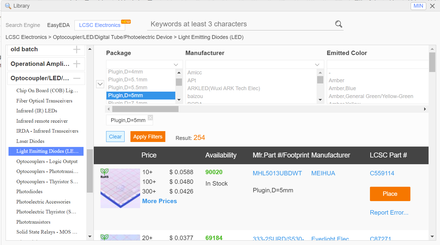
For today, I’ll provide the product codes I used below:
- Battery Holder: C70376
- Button: C110153
- Resistor: C58608
- LED: C2164
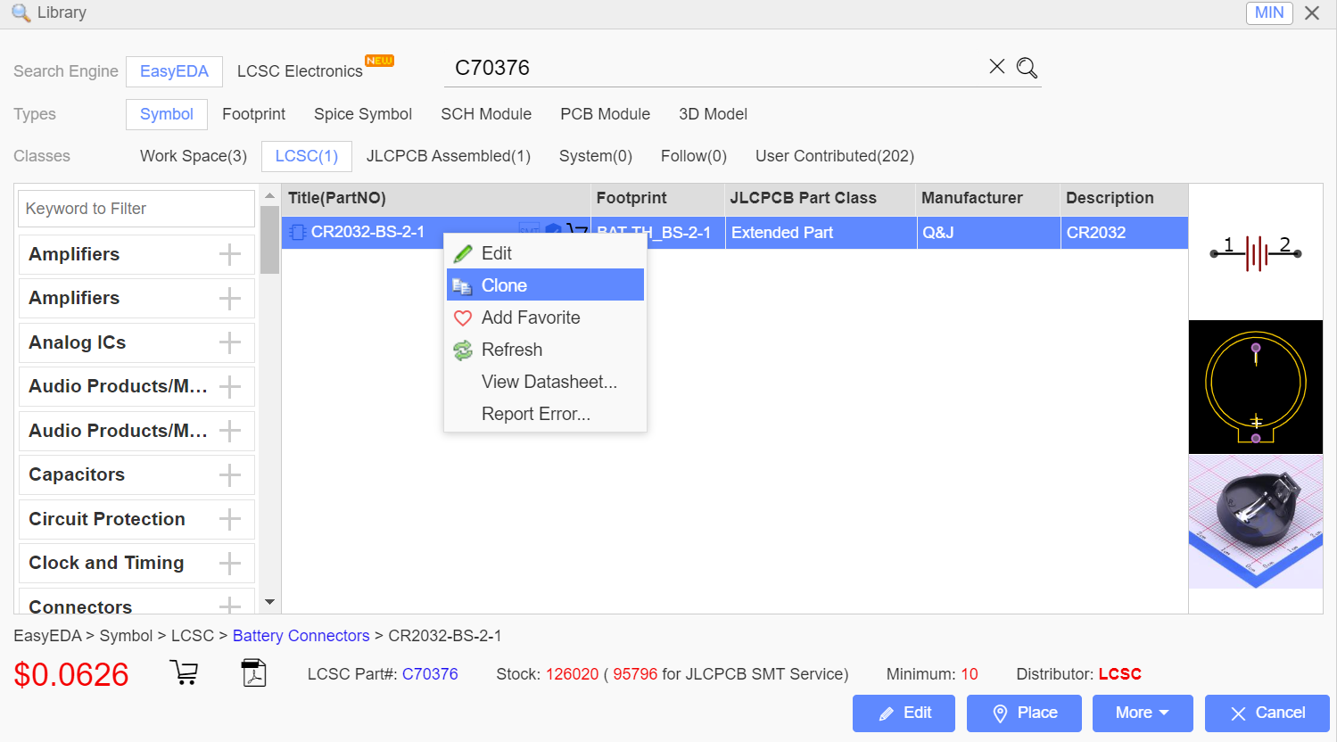
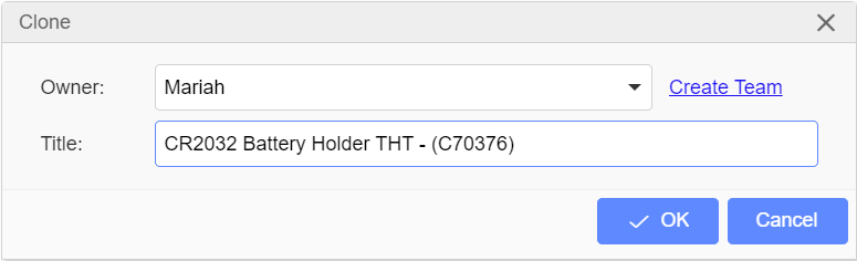
What’s super useful is that you are able to ‘Clone’, rename, and save components to your own personal library to have on hand the next time you need them! I tend to give it a common name that I use for the part, whether or not it is THT or SMT (through-hole technology, which pokes through the board and is soldered on the backside, or surface-mount technology, which rests on the face of the board and is soldered to pads on that side), and the LCSC product code. That’s just what I do, but you’re welcome to do what works best for you!
Go ahead and place each of the parts we’re working with into your schematic!
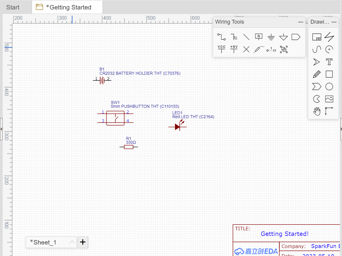
Yay! We have all our little buddies, ready to go! Let’s rearrange them a bit to make our connections a little easier (think of this as your “breadboarding stage”, it’s a very similar process):
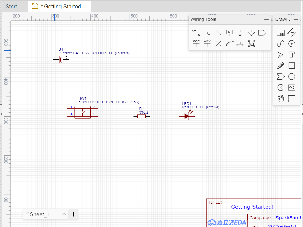
You may be wondering, “Mariah, why the heck is the battery so far away from everything else? Don’t we need it to power this whole thing?” Yes, we do! So, let’s talk about that: we could run all of our connections to the battery as we would on a breadboard, but in a more complicated circuit that would become a lot of things needing to connect to power and really bundle up our schematic.
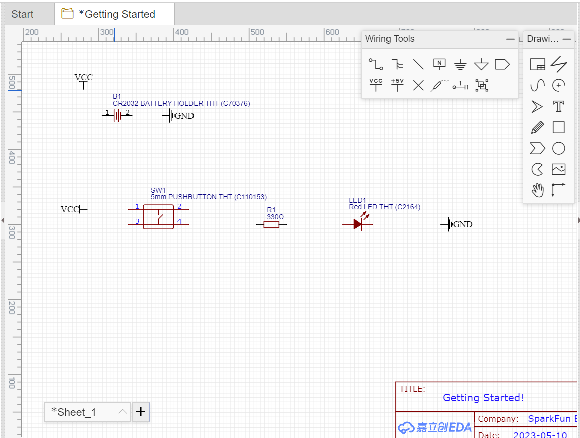
So, what do we do? Well, similar to using power and ground rails on a breadboard for things to connect back to, we have VCC and GND flags for our schematic. Flags are a handy tool that allow us to make connections on a schematic without having to draw it all the way out; so as long as our battery is connected to VCC and GND, everything else that is connected to one of those flags will be connected to our battery!
Go ahead and grab, first, the VCC flag from the ‘Wiring Tools’ bar; we’ll place one by our battery, and one by our button (this will allow us to control when power goes from the battery to the LED with the button). Next, we’ll grab the GND flag and place one on the other side of the battery, and one on the far side of the LED, like so:
Now all that’s left is to make our connections! The ‘Z’ looking shape with a circle on each end is our wire tool, which you can also access by pressing ‘W’ (use the ESC key to exit the tool). To make sure you’re connecting things, hover over the part until you see a little circle pop up; this is to indicate that the wire you’re drawing is to be attached to that part.

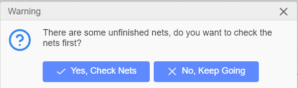
And with that, we’ve completed our first schematic diagram! Here comes the super fun part: at the top of your screen, hover over the ‘Design’ option and select ‘Convert Schematic to PCB’. This will trigger a popup that asks if you want to ‘Check Nets’; essentially what that does is say, “Hey! You have some unused connections in your diagram!” But we don’t want to use every possible connection available on our components, although it may be nice to double check that we did indeed make the ones we meant to. If you’d like to see that process, go ahead and allow it to run, otherwise we’ll say, “No, thanks!” and move on. Another window will popup and ask lots of questions that we don’t need to worry about for our purposes today, so just exit out of that.
This is the PCB design space! The pink rectangle you see is our board outline and will be the size and shape of our finished board; this is auto-generated based on the size and number of components we have, and can be customized! But we’ll stick with this for now. You may also notice the blue lines criss-crossing over our parts; these are called “Rat’s Nest Lines” and show us how we wanted things connected based on our schematic diagram.
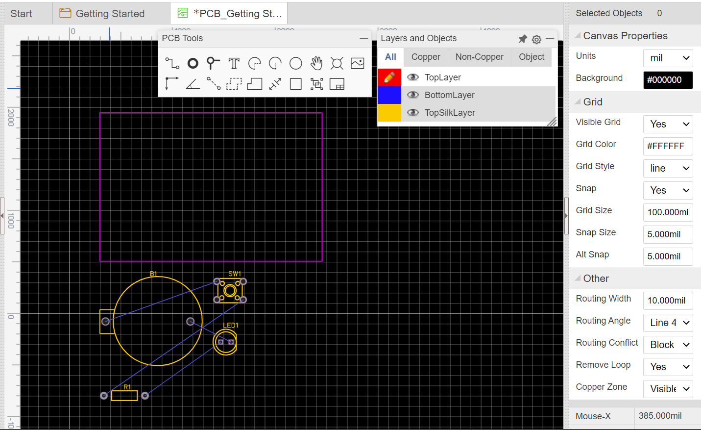
However, before we can start doing that, we need to lay out our components how we want them on our board. I liked this setup with the battery on the left and our button and light on the right, but you can do whatever you like (use ‘R’ to rotate components)!
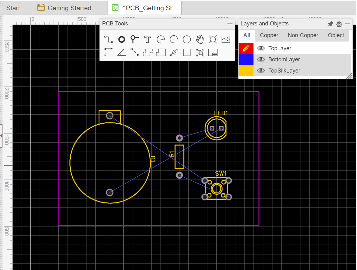
Now that things are where we want them to be, we can start making our connections! Just like on the schematic, you can either select the wire tool from the toolbar, or press ‘W’ as a shortcut (make sure that you have ‘Top Layer’ selected under the ‘Layers and Objects’ menu). Then we just select whatever pad we want to start with, and that Rat’s Nest Line will highlight, letting us know where it needs to connect next! I started by connecting the battery to the button, and the resistor to the LED.
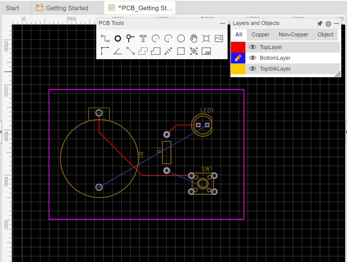
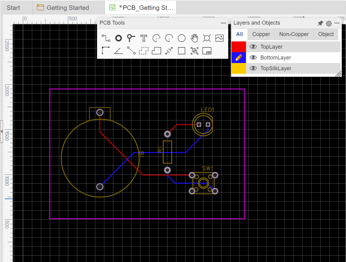
You may notice here that the last couple connections are intersecting with the traces we’ve just made; this isn’t great because crossed traces means crossed connections, and that means a dud board or even short-circuiting. So, what should we do? There’s two options: we could go alllllll the way around our current traces to connect the last Rat’s Nest Lines, or we could do something fancy.
Under the ‘Layers and Objects’ menu, select the blue square where it says ‘Bottom Layer’; this will allow us to create traces on the other side of the board, going safely under our existing top layer traces! This is a benefit to designing with THT in that, since the components go through the board, they can be accessed by traces from both the top and bottom.
And that’s all of our connections made! You’ve just designed a fully functional PCB for the first time! Let’s take one last look at something before we go, and that’s the ‘Top Silk Layer’, or the yellow option on the ‘Layers and Objects’ menu. I wasn’t a big fan of where the component IDs were placed on this layer, so I decided to change those up a bit.
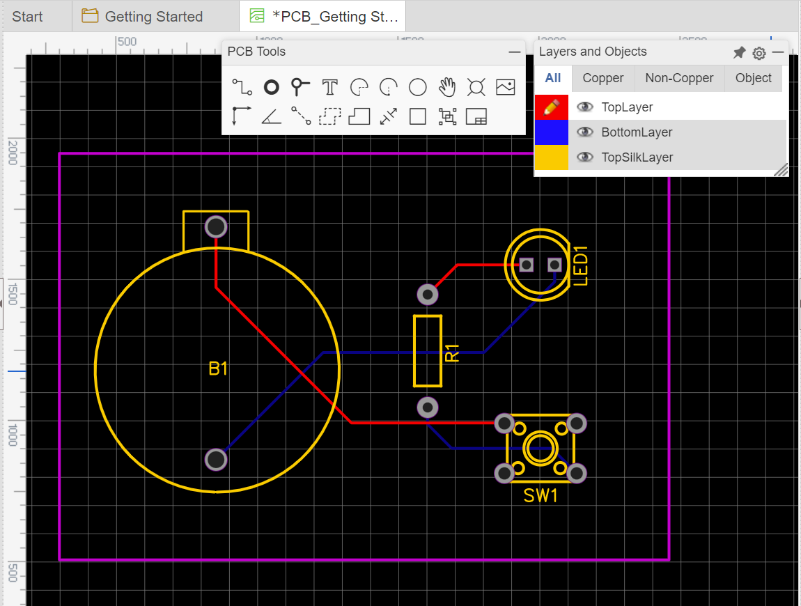
Now, not only can we manipulate existing silk layer text, but we can create our own! With ‘Top Silk Layer’ active, select the ‘T’ tool from the ‘PCB Tools’ menu; this will generate ‘TEXT’ that we can change to say whatever we like.


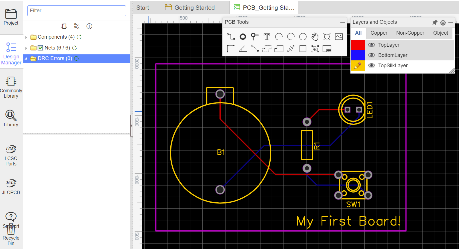
If we had a more complicated circuit, it may be hard to tell if we’ve done all we meant to. One way to check on that is to hover over the ‘Design’ tab at the top, and select ‘Check DRC’ (DRC stands for ‘Design Rules Check’ which looks for things like crossed traces, missed connections, and so on).
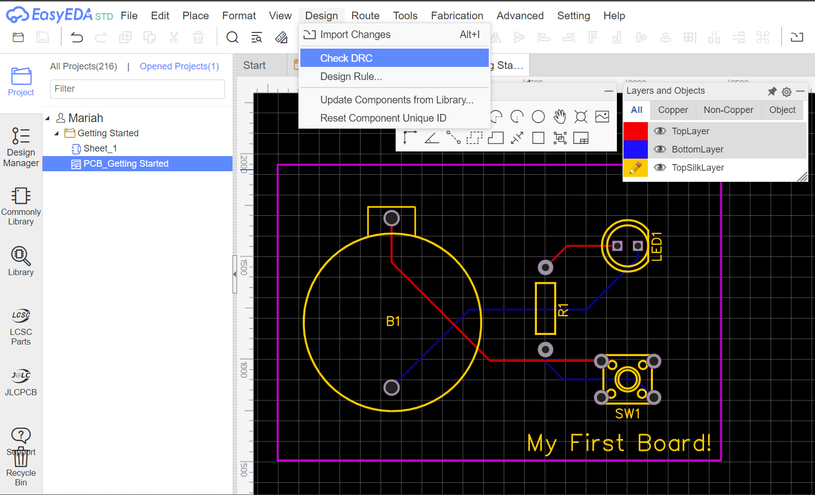
As you can see on the left, we have no DRC errors, all of the components we wanted, and we’ve made every connection that we laid out on our schematic diagram!
That’s all there is to it! Your board is ready to be manufactured! But what color should it be? If only there was a way to visualize what it might look like… Well, guess what? There is!! Hover over the ‘View’ tab at the top of the screen, and select ‘3D View’; this will create a virtual PCB based on our design!

From here we can manipulate the characteristics of our board, such as the color and pad types. It starts out blue, but I really like the red and black the best (the black color option comes in a matte rather than gloss like the others), so I’m gonna change it to red; check out each of the color options and choose your favorite!
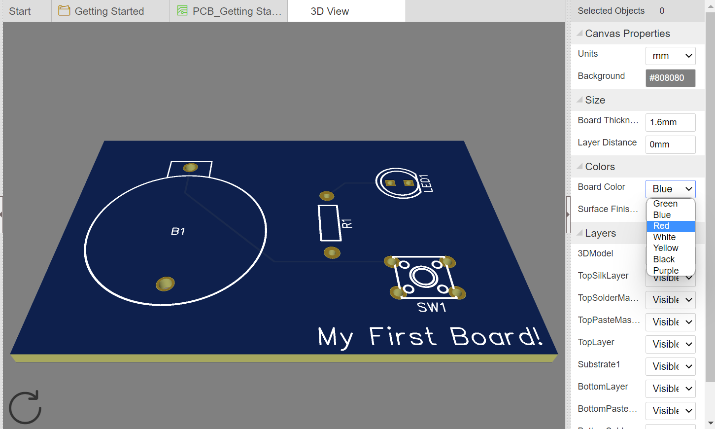
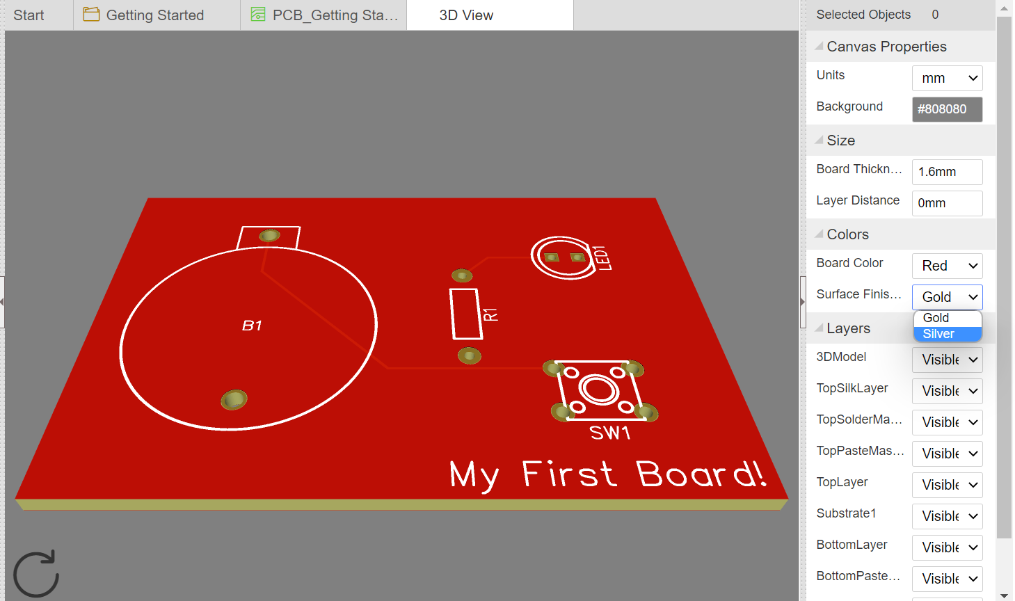
Since this is a 3D view, we can even rotate our board around and check out how the back looks; here we can even see the bottom layer traces that we made!

That’s so fun! How can I learn more?
I’m so excited to get to share this process with y’all; creating PCBs is one of my favorite things to do and I encourage you to play around with this program. Keep an eye out for the next installment of this mini-series where I’ll walk you through designing with surface-mount technology! And please share your PCB projects with us, and let me know if you have any questions or would like to see something specific moving forward, and I’ll do my best to provide answers and/or examples; welcome to the wide world of PCB design!
Leave a comment below, or find us on Twitter, Instagram, Facebook or LinkedIn.


Easy EDA does some wacky things if your doing a double sided board and you place different components on the same X and Y but on different layers. Puts one of the components on the same side when you generate the gerber.
One quick question that I didn't see answered in the above: Is it possible to get this to create Gerber files for the newly designed board? (For the un-initiated, most of the companies that actually manufacture boards will accept Gerber files. With >50 years in electronics, I'd guesstimate that around 95% of all electronic gadgets have, at some point, been Gerber files.)
Thanks to sometimes flakey Internet connections, I'll probably stick to using KiCad. But it's good to see another option!
BTW, I recall an incident maybe 20 years ago at an Amateur Radio club meeting where one guy was proposing a circuit for putting on several remote sites, including some mountain tops. He was proposing to built them with "point to point" wiring -- I piped up and said that I thought it would be an ideal situation to create a custom PCB. You should have seen the "deer in the headlights" look on his face! (IIRC the circuit would have involved about 20 components -- I don't even recall there being one with more than 4 pins, so it would have been relatively easy.)
Great question! Yes, there is: at the top right-hand side of the designer you'll find a little file icon with a "G" on it that will allow you to generate and download the Gerber file for your board.
I've heard of KiCad but haven't had the chance to play around with it yet; definitely on my list of cool things to check out!
In addition to KiCad, I've also used gEDA and [been ab]used [by] Eagle. gEDA was an "open source" solution, mainly used on Linux, but last I checked it hadn't had any updates in many years. About 10 years ago, I worked for a small "start-up" company that used Eagle -- which I found to be awkward to use, to the point that I felt that rather than "using it" I was "being abused by it". I think that KiCad is a much more pleasant experience than Eagle.
One thing I will caution folks on: before actually having your PCB manufactured, check the "pinouts" on EVERY device -- libraries do contain some errors! Years ago, I assumed that something like a 2N2222 transistor would have a correct footprint. When the circuit didn't work, I tracked it down to a miswired transistor -- I was able to get it to work by twisting the leads, but it sure looked like the transistor was desperately needing to go to the restroom!