- Home
- Product Categories
- Prototyping Boards
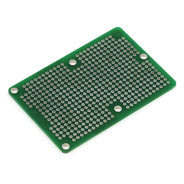
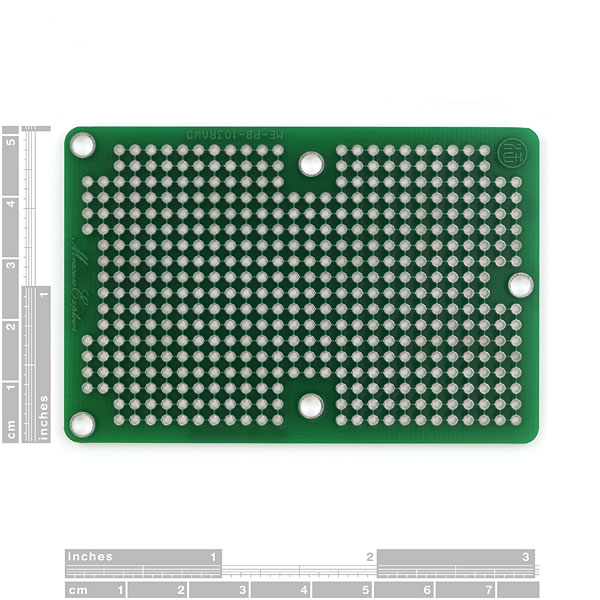
- ProtoBoard - Rectangle Wired 3"

ProtoBoard - Rectangle Wired 3"
This is a different kind of perf board. 3" long and 2" wide, the holes are plated through and PCB is double sided like you would expect. All holes are routed together on both sides. The really neat thing about this board is every pad has a 20mil width trace connecting to every other pad. Every pad is shorted together! This actually speeds up prototyping because instead of having to wire from one point to another, you simply cut the traces to isolate the route or pad you want to use. Your board will look a lot better and be more robust without lots of point to point wires to interfere. Standard 0.1" spacing with a 4-40 (3mm) holes for mounting. Great for quickly prototyping stackable circuits.
ProtoBoard - Rectangle Wired 3" Product Help and Resources
Soil moisture-sensing by hacking a solar light
June 19, 2014
How to take a solar powered pathway light from a hardware store and make it into a crude soil moisture sensor.
Core Skill: Soldering
This skill defines how difficult the soldering is on a particular product. It might be a couple simple solder joints, or require special reflow tools.
Skill Level: Noob - Some basic soldering is required, but it is limited to a just a few pins, basic through-hole soldering, and couple (if any) polarized components. A basic soldering iron is all you should need.
See all skill levels
Comments
Looking for answers to technical questions?
We welcome your comments and suggestions below. However, if you are looking for solutions to technical questions please see our Technical Assistance page.
Customer Reviews
No reviews yet.
Nice idea, terrible implementation.
The traces are on both sides of the board and you have to cut the same trace on both sides.
As pointed out by another poster here, having the traces on both sides gives no advantage since its still effectively a one layer board. Paths cannot cross without shorting, so its mandatory to cut the traces on both sides.
And, when you flip the board over to cut the opposite trace you are looking at the mirror image of the circuit so it is difficult and error prone to locate the correct trace.
Also the traces require significant effort to cut with a utility knife. Once you have components on the board it will be even harder since it won't lie flat on a surface. Furthermore if you forget to cut a trace before mounting a component, you will have to desolder it because the traces are covered by the component (such as an IC).
Finally, implicit connections are less obvious than wired ones, so expect to spend a lot of time double checking your work.
Expect to spend lots of time with a multimeter testing connectivity at every step.
Many of these problems would be fixed by putting the traces only on one side. Also I would prefer if there were fewer builtin traces, rather than fully connecting every via, it would be better if most of the connections were only in one direction.
Cutting traces is more reliably done with a Dremel and one of the tiny engraving cutters, like this: http://amzn.com/B00008Z9ZT
You could also just cut all connections on the top
You could indeed. The spirit of the comment is that you shouldn't have to.
You can see this board in action on our blog at: http://arduinofun.com/blog/2009/01/04/lars-vers10-build1/
These boards are great! We used colored sharpie markers to mark out our holes rather than printing off a PDF file. Keeps you sane!
I found these boards very difficult to use. They would work very well with a lot of planning and would cut down on the need for jumper wires, but I was constantly cutting the wrong jumpers when I flipped the board over. It would be easier to use if the board was single sided.
SPARKFUN!!! You need to make these with only one side traced and make smaller or larger versions of this board, yes I do want to get this and not have a wiry mess but then again this whole double side trace thing is just stupid. and this is wayyy to big for my project. maybe like half the size would be nice and yes, I know, I could use a saw but then it wouldn't look as neat before I cut it. REASONS LIKE A BOSS!
Highly Recommend. These boards are great! My son and I are just getting started learning about the Arduino and these made creating a shield fast and easy. I agree with the other poster that some bigger boards are needed as well. It would also be nice if there was one designed to fit the Arduino a little better by doing away with the 2 center screw holes.
How'd you cut the traces?
Thanx,
Chill_Bill
Use an exacto knife.
Does this item still have traces on both sides? I would rather not buy it if that is the case...
I am really unhappy with these boards. I bough three of them to use in a project I was working on and after cutting half of the traces I needed on one board I just became frustrated and gave up. Bought some regular protoboard from Radio Shack instead. I dont know how some people get these things to work properly. I've dulled two exacto blades just trying to cut the traces I need for one board and I still had two more to do.
I ordered these by mistake, and they are difficult to use. Especially with traces connecting the pads together are on both sides of the board. The 08815 is much easier to use with an unconnected plane on one side, which makes for a good ground plane.
Someone tell me how you’re supposed to use this… I think I need one but I don’t know how to use these.
I'm sorry, but these boards are a gimmick at best. I bought this double sided PCB expecting a double sided PCB. Instead, I got a board full of vias. This means that instead of being able to have a board that's quick to prototype with and which allows for overlapping traces, you have a board that requires jumpers for overlapping traces and double the cutting (since you have to cut the traces on both sides).
I guess my question is this: what's the point of making this double sided?
For some customers, the wired board does actually increase their prototyping time. I think you were probably looking for this double-sided protoboard instead. Sorry for the confusion!
Any idea what kind of current the traces can handle?
From eyeballing the width and length, I would guess 1A. Calculator.
i just opened the package and think i may regret this purchase already... thought it would save me time with the traces... i think, now, it will take more time cutting every trace on the top side....
...and extra blades for lots of cutting
https://www.sparkfun.com/products/10325
HERE IS HOW TO CUT THE TRACES PROPERLY: simple hobby knife (link below). Check the connections w/voltmeter on Ohm-setting. Only thing that worked easily for me. You don't need to go rambo, just a few runs of the blade, and an ohm-meter check.
https://www.sparkfun.com/products/9200
These boards are THE BIGGEST HASSLE. The connections between the pins are very difficult to break. It would be much faster to use the ProtoBoard - Rectangle 3" that just has the traditional individual pads. Yes, you have to solder in wires to make connections, but it's a lot easier and much less frustrating than having to break the connections on this board.
When I got this board I thought that it was ridiculous to think I could easily cut all these traces. 15 minutes with a voltmeter, sharpie and a hobby knife and I was in business. Very happy with this!
Is this the only wired prototype board available anywhere?
Hey there sparkfun. TY for these things, they're great and all, but I was wondering if you guys might come out with a line of them that are about 4"x 3" (maybe 4x2) with straight corner holes. No offence, but the offset center holes on the side, and the single hole towards the end kinda get in the way of some projects. Also like many others have said here, having the double sided tracing really makes it a hassle having to flip the thing over and recut every trace (backwards this time) to get it right, (I've actually found running my sander over this for a few mins taking all of 1 side off is better int eh long run). I don't mind cuttign the traces, no prob there. But like another mentioned, a horizontally traced breadboard-esque version (with space in the center for DIP Chips) would be pretty nifty IMO (and would be a big help on my next few projects.) Well I'm just saying, you know, something to think about.
Maybe it's just me but this board is not worth the hassle. It takes way too long to do the layout and cut the traces. The double sided plating is useless since the holes connect each side of the plating which prevents you from crossing tracks.
This sure sounded like a neat idea, but I hated it. Really tedious to try to get the cuts the same top and bottom, and I gave up partway into it simply because I had no confidence that I was going to make a working circuit, and did not want to try to debug this thing. Skip this and stick with an old school board.
I would love it if you had some of your smaller boards, like the 1" round, made this way, too. Another variation might be a board with room for a single 14pin DIP that's broken out with the holes connected like this one. That would be great for many of my smaller projects.
I got a couple of these, but have always been daunted by the amount of work needed to actually put a project on one. The problem is that I don't want to waste a lot of space, so I want to use as much of the 3" board as possible, but that means a LOT of work cutting traces.
I think Adafruit has a great idea with their boards which are set up exactly like a breadboard, but have plated through holes, which are all connected as they would be on a breadboard. There's still plenty of room for a board with pre-run traces, but don't plate through the holes and just to horizontal on one side and vertical on the other. Perhaps set up dedicated bus strips with plated through holes.
I (edit: REALLY) want a version that only has the pads on the horizontal rows shorted. Then it would be like a thin, solder-able breadboard! :D
EDIT: And RadioShack has one! Along with a bunch of other components SF doesn't have. It's embarrassing buying from there, the clerk sees a kid buying breadboards and searching for the right transistor in the parts drawers, and you know they're thinking "That tween doesn't know what he's doing.". And I feel bad buying from there because they're not SparkFun.
Chill_Bill, I wouldn't worry about looking clueless at Radio Shack. The staff there usually don't even know what those components are; they just stock the shelves. Whenever I'm there I just tell sales people that I'm looking for components and they leave me alone and try to sell a cell phone to someone else. Plus, you'll always be clueless at something (many things, really), but at least you're actively learning new stuff.
This exactly.
i just finished with my first small project with this board and i am happy with the results. i created a breakout board for my paralax propeller with 2 eeproms (with jumpers to select which is 0) and a logic level converter (for programming through an unchipped arduino).
the 2-sided thing maybe annoying sometimes but they did save me from using more jumper wires when i accidentially cut a few routes too many on one side.
its best to make nice deap cuts while carving your circuit. it has occured to me that while soldering a 8-pin socket one of the routes shorted and i had to remove the socket again.
anyway im glad with this protoboard and im looking forward to create a tellymate on one of these
it took me 2 days of work to cut all the traces for my project. i was using the dremel engraver tool that pstemari suggested, but it quickly became dull and unusable. i ended up just using a cutoff disk. i still need to bore out the plated holes everywhere that top overlaps bottom. considering the time invested and the extra 15 bucks i spent on dremel bits, it might just be cheaper to have one cut with patchpcb.
i ordered one of these to reduce the size of an rc reciever that i designed using an arduino and a breadboard, and other components. currently trying to cram as much stuff onto it as possible, essential parts first and then as many extra headers as i can add for servos and other stuff..
of course the plated though holes may be an issue. im thinking i may be able to very carefully drill out the plating, thus eliminating the via. so long as i dont solder anything to either side this should work to isolate top from bottom in some spots. i wanted to get a schmartboard for this project, but couldn't find a distributor that can ship to alaska on the cheap (thank you for using the us postal service, don't ever change that and i'll keep buying from you). i saw this one and thought it would make a cheap if not ideal alternative.
Im sorry to say, but this was useless to me.
Wouldn't fit any enclosures I had available without needing to cut it in half. Part of why I hate the hack shack. Should have bought the enclosure here.
sounds like the problem isn't that traces are on both sides, but that the board has solder mask. cutting through traces is easy, but cutting through solder mask is a pain in the ass. use a sharp xacto and put some elbow grease into it. also try cutting with the trace to loosen up the solder mask.
traces on both sides makes it possible to do 2-sided designs if you actually design it and do the layout on paper first. a single sided version would still be useful though.
These things are useless. Tried to cut the traces with a utility knife, edge of a jewelers file, and a small pair of SHARP wire cutters. I tried to isolate a 4 hole by 4 hole square, and finally gave up. I agree that they are too time consuming, don't work as advertised (on Ebay), and are a waste of money. Save your frustration and do it the old school way, with wires!
It seems like some people are suggesting cutting traces with a sharpie? I can only imagine that they're using an etchant or other chemicals of some kind.
I thought this board would be really cool, but instead, cutting traces with an exacto knife is a giant pain in the ass.
Maybe traces horizontally on one side and vertically on the other? or does that just complicate it way more. LOL
The plated-through holes defeat that.
Without plated through holes, you could isolate any simple connection with six cuts, and corners would require two cuts and a feed-through to switch sides.
However, with the holes plated through, while two cuts isolate the connection on one side, every hole it crosses connects to the trace at right angles on the opposite side.
What would be good is a set of traces mimicking a standard prototyping socket--rows of five pins separated by .3", and columns between running end to end for power buses. Standard DIP chips straddle the buses, and if you really want to be elegant, you make provisions for a 0.1 uF bypass cap every eight rows and a 10 uF cap at the ends of the columns.
this is a great idea, but i did not realize until i got it home that it had plated through holes. it may as well be a one sided board, since connections on opposite sides cannot cross. this means you have to cut the same pattern on both sides. The extra expense of making it double sided also doubles the work with no increase in performance.
you could just cut around the whole pad on one side where you want that pin to trace on the other side
oh and forgot a diagram for planning can be found here: http://cgi.ebay.com/ME-PB-103SW-wireless-circuit-proto-prototype-PCB-board_W0QQitemZ300327800181QQcmdZViewItemQQptZLH_DefaultDomain_0?hash=item45ecee8d75#ht_3248wt_903
I like the idea, but I used this board for a project and the process of cutting the traces was extremely time consuming. I have to say that, based on my experience, running wire is faster than going through the trouble to cut all the traces.
Can someone tell me if the wiring is on both sides or one side only ?
Andrew
The wiring is on both sides. Don't be fooled into thinking you can get too tricky with the layout ( I did this ), every hole is essentially a via connecting both sides.
The best way I found to cut the traces was a steel ruler and a break-away blade. Focus on getting a clean score first, then gently work the blade back and forth in the groove to break them. I found it a lot more efficient to cut them in groups than to attack single trace points.
The end result is really clean and impressive
What is the best method for cutting the traces?
OK, Figured I can flatbed scan one of these boards and create a Pdf of the layout and see how that work out. Otherwise maybe I'll make one in eagle or other pcd application and put it into a Pdf. Will provide a link on Sparkfun's forum when done.
Firstly, Great Product.
I would have to agree with previous poster for a Pdf of the board for layout sketching.
Also, bigger is better. How about a larger board, with maybe some smd (soic ?) pads connected by the 20 mil traces to the plated thru holes? Not for the smaller board but for a larger sized one. Maybe a layout similar to the Diprotodon Protoboard or add this design to the Diprotodon instead.
Supply .pdf of pad layout so users can use pencil to layout traces and component layout
out of stock :(
I was just about to make some of these as an experiment in batchpcb! now I don`t have to =)