
Beginning Embedded Electronics - 9
Lecture 9 - Eagle: PCB Layout
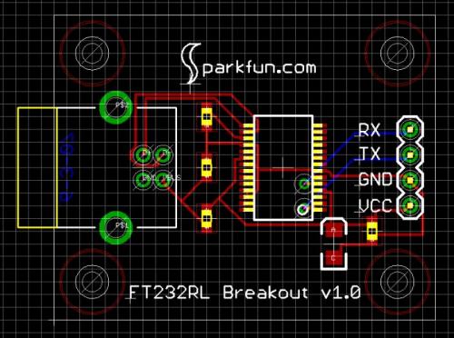
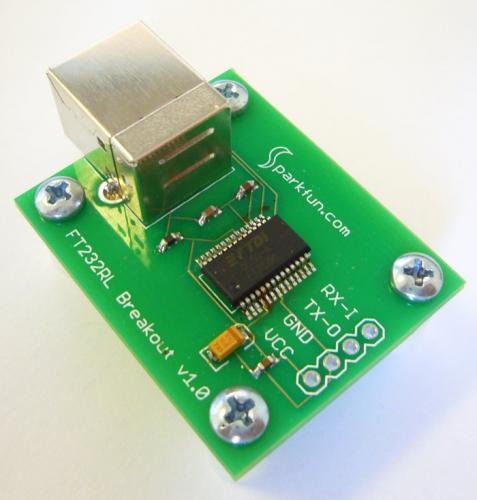
To learn how to use Eagle, we are going to create a simple breakout board for a popular USB IC. The FT232RL is a USB to TTL serial converter. This section covers the physical layout of the PCB.
We've got the schematic captured and the connections should be made correctly. The next step is to arrange various components on a board and then send the board files out to a manufacturer (also called a fabrication or 'fab' house).
Layout is an art and engineers make bad artists. It's all about the small polishing - text labels, stand off holes, correct footprints. Just keep turning out PCBs and you'll see your layouts improve dramatically with practice.
Before you do anything, turn on vector fonts! If you don't, your silkscreen text will be off on every PCB you create:

From the Eagle control panel, click Options->User Interface
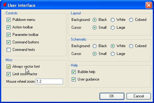
Select 'Always vector font'.
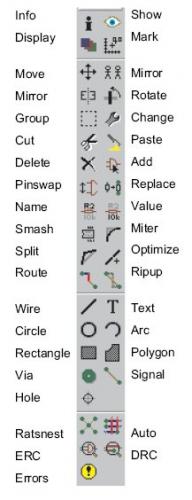
Above is a breakdown of all the different buttons in the Layout window. You can view the name of each button by hovering over the button with your mouse. Many of the short-cuts from the Schematic window still apply:
-
Press escape at any time to stop the current action and return to the Layout window
-
F7 to move a part
-
Alt+F7 to group a bunch together
-
F3 to delete a part
-
F4 to rename a part (change C7 to C2)
-
F5 to re-value a part (change 0.1uF to 10uF, etc)
-
F6 to smash a part (be able to move the name and value tags)
-
F9 to start routing a wire
-
Alt+F9 to rip up a wire
If you get this error while moving bits around:
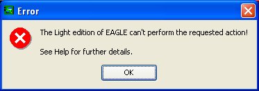
This just means that you are trying to put a component outside of the allowed area. With the Light edition of Eagle, you can only place components in quadrant I (upper right quadrant), whereas the components show up by default in quadrant II (upper left quadrant). Just move the parts to a positive X and Y coordinate and you should be ok.
Starting with our current layout:
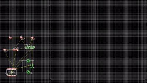
The first thing to do is correct the board outline. I don't know why Eagle slightly offsets the default border.
Make sure you're on a 0.1" grid by pressing F10. Then hit F7 and hold control while clicking near the origin. This will grab the frame corner and force it onto the 0.1" grid. Make the bottom left corner sit at (0,0):
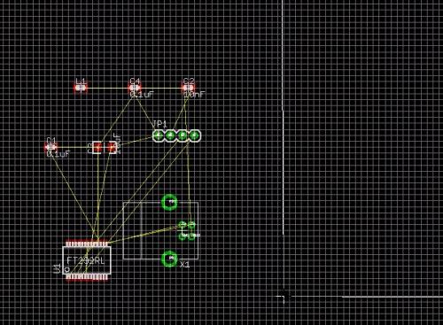
Do this for the other three corners bringing them in to make a 1.5x1.0" square board size.
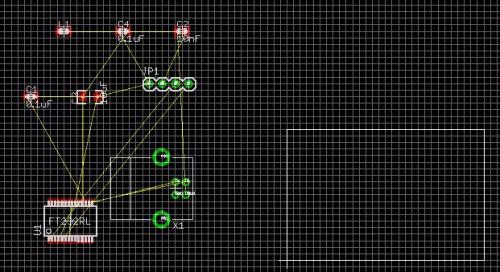
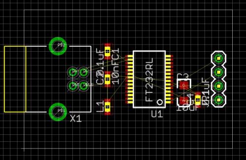
Now go to town bringing the components into the board area. Keep in mind the gold color un-routed 'air' wires. The less twisted you make these by creatively arranging your components, the easier the trace routing will be.
Remember:
-
Press F7 to move a component
-
Right click to rotate
-
Hold control to grab a component at its origin
-
Scroll wheel to zoom in/out
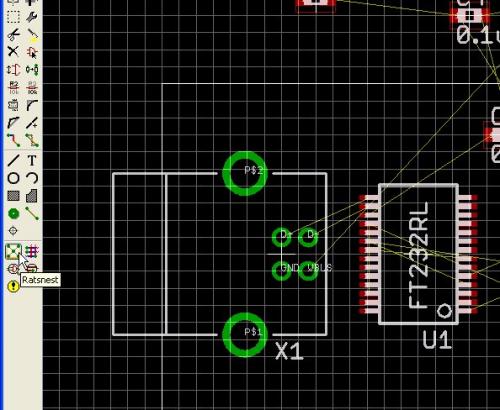
Hit the Ratsnest button from time to time to recalculate the air wires.
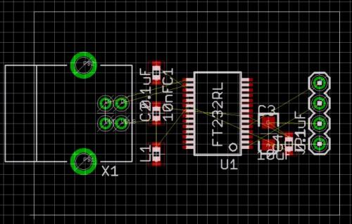
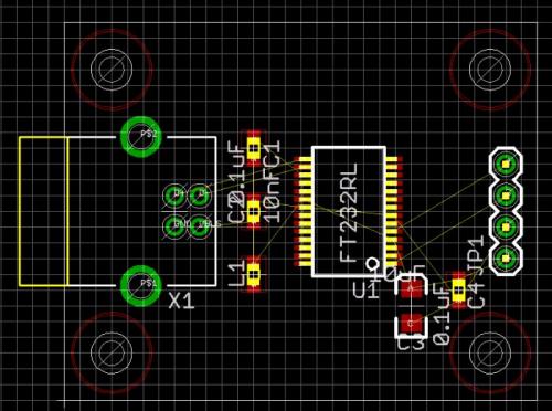
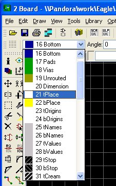
Here are the components arranged in a basic configuration. Another beef I have with Eagle is the default colors for the various layers make it impossible to see what is going to be printed on the silkscreen layer. Let's change the 'tPlace' layer to pure white and change the 'tDocu' layer to lemon yellow.
Click on the 'Display' button, scroll down to layer 51 and double click on the gray box next to 'tDocu':
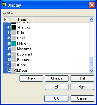
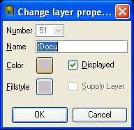
Then click on the gray 'Color' box and change it to something interesting like lemon yellow, then click ok. Anything you do on this layer will now be yellow. Do the same for layer 21 'tPlace'.
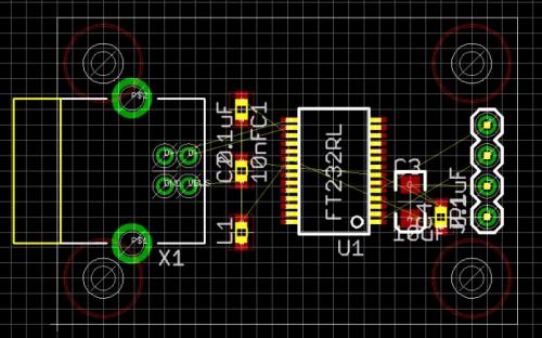
Now this is starting to make sense! Anything in yellow is just there to indicate physical size. The yellow part of the USB connector is only there to indicate that the connector sticks over the edge that far. Only the white part of the USB connector footprint will actually show up on the silkscreen print on our PCB. Anything in light gray (tNames and tValues layers) will not print on the silkscreen layer. They're just there for your own reference. We can of course change how the various layers are processed (and include the value and name layers on the silkscreen) but this can cause a lot of squeezing and hassle. It's up to you and your design but we will leave the part indicators and values out of this layout.
The next thing we need to do, for all PCB layouts, is to add stand-off holes. These holes will allow you to insert a simple screw and hold a stand-off in place. Without standoffs, PCBs will sit uneven against a flat surface (because of the bumpy solder joints protruding on the bottom of the board). Having a PCB sit flat against a surface is also a bad idea electrically - I've sent $200 up in smoke because some bits of clipped wire shorted against the bottom of my board when I was troubleshooting it.
I like to use 4-40 screws and 0.25" diameter plastic standoffs on everything. These 4-40 screws need a 0.13" diameter hole and the standoffs have a 0.25" outside diameter that we will need to take into account. If you have not already done so, add four of the 'Stand-Off' components to the schematic (and therefore PCB). This component was created to couple the 0.13" drill with a keepout ring. This keepout ring helps show were the screw head will fall. If you fail to take this keepout layer into account, the screw will go through the hole, but the screw head may run into or short components.
Throw four standoff holes around the corners of your board.
Ahah! Now I see why I made that keepout circle. You can see where the standoffs would have run into the USB connector. Looks like we've got some bumping to do...
By using the group (Alt+F7) and the move (F7) commands, I increased the border to 1.5x1.2" which is a bit bigger than I would like, but for the purposes of this tutorial, we're not going to stress tight packing of components - rather we want to stress the basics for a good PCB. Notice how I flipped and dropped C3 and C4 down a bit? Time to add labels!
A 'C2' label is handy when you're populating a board or when you're troubleshooting a complex circuit, but on a day to day basis, you probably won't need to know where C2 is. On the other hand, the TX and RX pins will probably be used every time you use the board! You really should label anything that will be connected to the outside world. To add a text label to a pin, click on the 'Text' button:
A window will pop up asking you what text you would like to add. Type 'TX' and press enter. You will notice that the text may be appearing on an odd layer. Be sure that you add text on the tPlace layer.
Drop down the layer menu and select tPlace for top silkscreen text
Once you've placed 'TX', press escape. Eagle will now show the text window again. Enter 'RX' and press enter. Repeat for RX, VCC, and GND. When done, press escape twice to return to the layout window.
In this case we have VCC/GND/TX/RX to label:
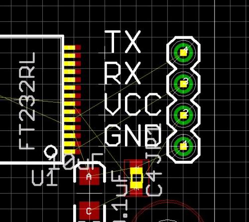
Make sure you add your labels to the 'tPlace' layer!
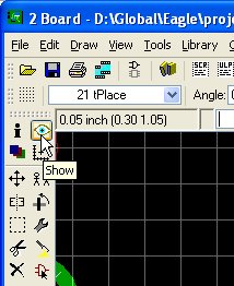
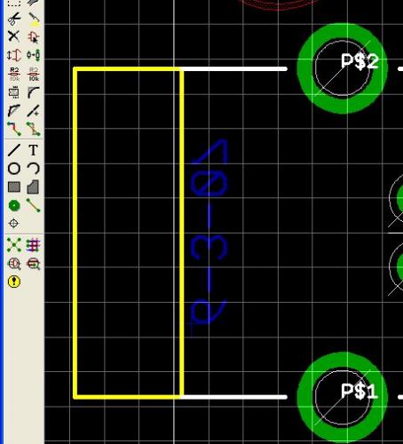
To check which pin is connected to which net, hit the eye button and click on a pin.
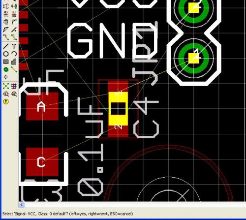
Checkout the text at the bottom of the Eagle window - pin 1 is VCC. Do this for all the pins and arrange the labels accordingly. You should also take the font size down to 0.05:
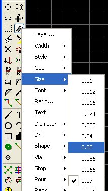
To change the font size, click on the Wrench ('Change' button), select 'Size', then 0.05. Now click on each text that you want to change the size on.
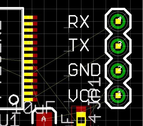
Labels in place and lined up
Try to get all the labels with the same vertical and horizontal alignment. This is a nit picky aesthetic thing, but it shows on the final board.
You will have many board revisions. It's always good to add a date code to the board so that you can match your files to the board version in hand. Add text to the bottom copper layer to an inconspicuous spot. The easiest way to do this is to add text to the top copper layer then hit the mirror button (you can also hit the scroll wheel on the mouse to move the component to a different layer). This will automatically mirror the text and drop it to the bottom layer.
6-3-07 mirrored, on the bottom copper layer, and underneath the USB connector. There shouldn't be any signal traces in this part of the board so we're not wasting space. You could add text to the bottom silkscreen layer but some fab houses don't allow bottom silkscreen (it adds an extra printing step).
Also add some text to the top silkscreen layer indicating what the board is, what it does, who made it, etc.
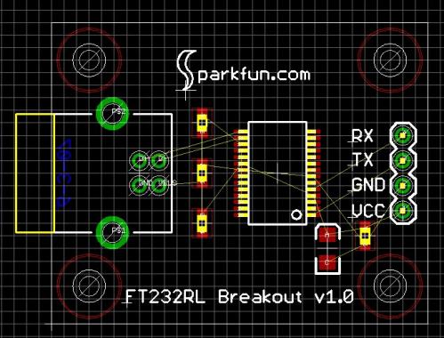
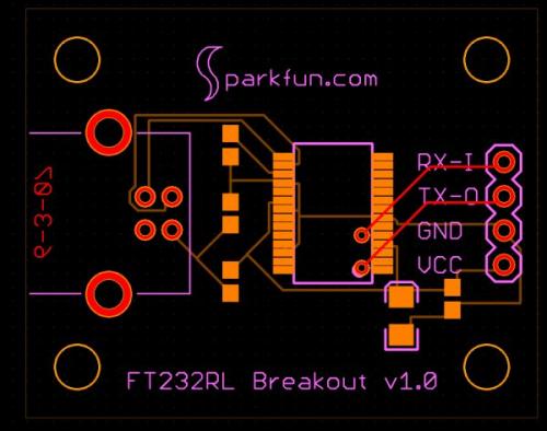
Above is the completed board ready for trace routing.
Many people swear up and down that an auto-router is a bad idea. It may be, but if we're not concerned about trace impedance or high speed signals, an auto-router is a great way to whip up protos. Spend your time innovating, not routing mundane traces.
To auto-route the board, click on the 'Auto' button. The defaults are all fine except for the 50mil grid:
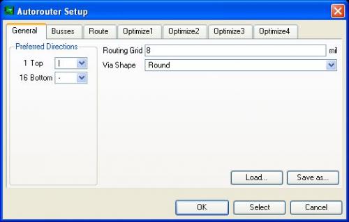
Change the Routing Grid to 8 (our fab house uses 8 mil traces and spaces).
Demo board auto-routed. Eagle files / PDF
It's not immaculate, but it will work just fine and the router took under 2 seconds to route. It would probably take me 5-10 minutes by hand. I will hand route sensitive parts of certain boards, but this is a very simple proto.
Things to check on every layout:
-
Date code
-
Silkscreen title and pin labels
-
Standoff holes
-
All connections routed
-
TX and RX routed correctly
-
Print off 1:1 and check footprints
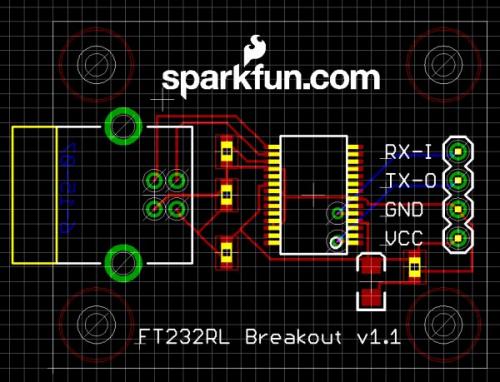
Routing TX and RX correctly? What does this mean? I can't tell you how many times I've heard newbies say 'well my PCB would have worked, but the manufacturer swapped the TX and RX pins'. No, the manufacturer did not swap them, the newbie neglected to actually read the datasheet (RTFD!). Sometimes an RX pin is an input. Sometimes an RX pin is an output. If you get it wrong, you'll look like a dunce. Read the datasheet and verify that everything is kosher. In the case of our FT232RL breakout, the TX pin is an output and RX pin is an input (pretty standard). I'm going to change the silkscreen indicators to read 'RX-I' and 'TX-O'. This should remove any doubt in my mind when I'm using the board a year from now - and so I don't have to go digging up the datasheet.
The last thing to check - print off 1:1 means to print on paper and 1 to 1 scale of the board layout. Then place the components on top the paper to verify that everything fits their associated footprint.
Another quick note about printing layouts - this can be a great way to create an assembly sheet. While you've got the PCB editor open, press Alt+F11. This will turn off all the layers that are not pertinent to assembly. Print this, I normally scale it up 3 times, and hand write in what parts go where. Quick and effective way to create a cheat sheet for PCB population. Pressing F11 will bring back the normal layers but you may want to activate/deactivate a few others.
Now that we've got the board laid out, stand-off holes in place, date code in place, and accurate pin labels, it's time to mash up the layers and create some gerber files.
What's a gerber?
There are lots of different layout packages out there (Protel, Orcad, Eagle, PCB, etc). One way or another all the PCB fab houses out there need a way to control their machines to work with your layout files. The universal format is something called Gerber Files. Basically these are txt files with coordinates that tell the PCB machines to go to location X,Y and do something (drill, expose, etch, print, etc). Because there are different layers to your PCB, you need to create different text files for the different layers. This is where the Eagle CAM program comes into play.
Once you're good and happy with your PCB layout (there is no turning back after you submit the files!), click on the CAM button to bring up the processor. This window will allow you to do different things to different layers. Eagle comes with a couple default *.cam files. The most common ones are the gerb274x.cam and excellon.cam. I got tired of running two seperate processors. I am also a hold over from Protel and a different naming convention so I created my own single file CAM processor. You can snag it here. The sfe-gerb274x.cam is based on the default Eagle file with a few tweaks:
-
Layers are renamed for easier reading - top copper, bottom silkscreen, etc.
-
All the mirroring is turned off - this will make gerber inspection much easier
-
A top paste layer was added in case you want to create a solder paste stencil
-
Excellon drill file is created along with the 6 magic layers
-
Drill file is 2:4 Leading (remember this!)
What are these magical layers you ask of? Anytime you transmit a PCB layout to a fab house, you need to pass them 7 files, and 7 files only:
-
Top Copper (GTL)
-
Top Soldermask (GTS)
-
Top Silkscreen (GTO)
-
Bottom Copper (GBL)
-
Bottom Soldermask (GBS)
-
Bottom Silkscreen (GBO)
-
Drill File (2:4 leading - remember this)
What is this GTL, GTS? These are the file extensions that the CAM processor will produce. A silkscreen is also called an 'overlay' (hence, GTO). And for your reference, a soldermask is also called a solder 'stop layer' because the soldermask prevents solder from being where it is not wanted.
Some fab houses will charge extra for a bottom silkscreen layer. You can just ignore this layer if you need to. You will also see a GTP file extension. This is the Gerber Top Paste file. You can use this file to get a solder paste stencil cut it you want. One would think that a GTP file would be the same as the GTS (top soldermask file). But no!
On the left, the soldermask layer. On the right, the top paste layer. The soldermask layer exposes the pads and the vias. You wouldn't want solder paste in vias! So the paste layer only has the SMD component pads exposed.
To create these layers, click on File->Open->Job

And select the sfe-gerb274x.cam file. Then click 'Process Job'. Some status bars will blink by, and within a few seconds, you should have a handful of extra files in your project directory:
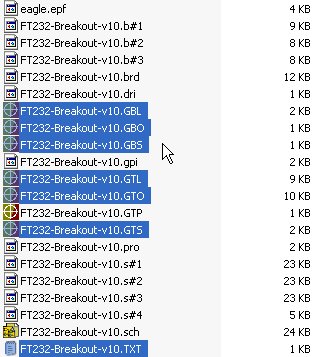
The magic 7 gerber files
Something I highly recommend is to review the gerber files before submitting them for fabrication. Viewing just what is going to the fab house can exposed potential problems that were shrouded before by all the extra layers and graphics in the Eagle layout window. There are some free viewers out there that will let you view the gerber layers together. Most of the free viewers require you to enter an email, require 15 seconds for them to advertise at you, limited to one layer, or other really annoying limitations. Luckily, Viewplot still exists. This free program will let you open and look at your layers easily and you don't have to fill out any silly forms to get to the download link! Be sure to select the drill file type '2:4 Leading' to matchup the holes to the layers.
Simple
But oh wait, what is that?
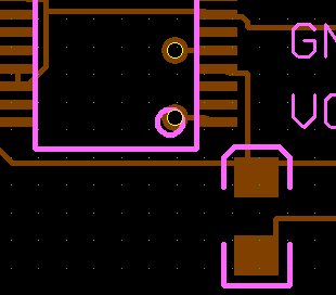
Silkscreen on top of a via
This silkscreen being broken up by the via is not a big deal. Mostly this is just to show how difficult it can be to detect problems from within the layout program. By viewing what you're actually submitting to the fab house, you can see exactly what they are going to deliver - be it good or bad. Review your gerber files before you submit! You'll save yourself time and monstrous amounts of money. If you want a $50 coaster, I'll sell you a truck full.
Zip these 7 files together and shoot them off to the fab house of your choice (Shameless Plug: we use BatchPCB). Depending on who you use and how deep your pockets are, you'll have to sit on your hands for 1 day up to 20 days. What do I do? I start other designs! While this board is being fabbed in 2 weeks, I create and submit a new design 7 days into it. That way I always have a new PCB proto coming in every few days. It's like Christmas every week! What am I getting this week? Is it going to work? I can't wait to test out my new cat tracker!
With the magic of television, I can jump 20 days into the future and show you...
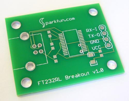
In the flesh
It looks great! Time to whip out some parts and the soldering iron.
Assemble your new board!
Soldering was not too bad. Silkscreen looks good. Standoffs look good. Time for testing!
Always assume a proto will short out the first time you use it. Be very cautious and be ready to kill power immediately. Plugging this board onto the computer - guess what happens?
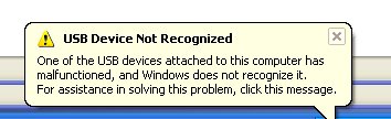
Uh-oh
What went wrong? Nothing is heating up. Nothing smoked or popped. The FT232 IC doesn't seem to be enumerating onto the USB bus. But why? Let's check the schematic one more time...
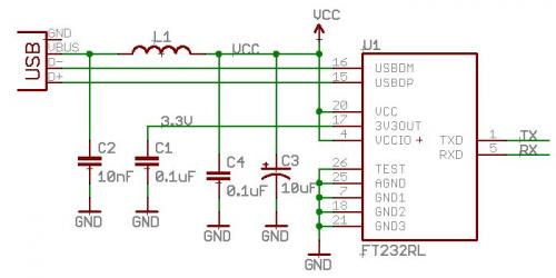
FT232 Breakout v1.0 Schematic
Son of a... This is why we prototype! Mistakes like this happens to the best of us. What is the problem you ask? Checkout the GND pin on the USB connector. It's not connected to anything. Without a ground connection to the board, no current can flow, the FT232RL will never enumerate. The board is shot! Or is it?
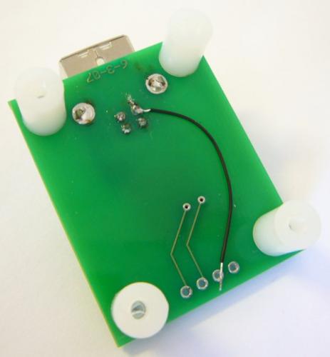
The green wire fix
(I know the wire is not green, but this is the nick-name for an oops! fix) This is my final thoughts on PCB layout - anyone can layout a PCB, but it takes a true magician to get a bad PCB working. Scratch, cut, splice, and otherwise modify your PCB until you get it working. This example was an easy fix. I've seen some really impressive fixes over the years.
From the SFE PCB History Museum
Don't immediately throw up your hands and layout a new board. Instead, make sure you get every bit of the functionality of your board working, by any means necessary, and then make all the revisions. Otherwise, you'll constantly spin your wheels with PCB revisions.
Things to remember:
-
Be sure to save your schematic as a new file name: *-v11
-
Be sure to update the date code on the board
-
Be sure to update the silkscreen on the board
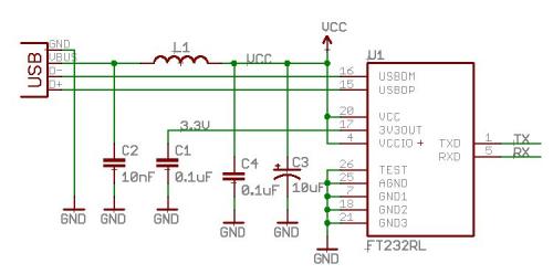
Updated v1.1 schematic with GND connection on the USB connector
Updated v1.1 board layout with new GND connection, updated silkscreen and date code
We love feedback! Please report typos, comments, or recommendations to spark@sparkfun.com.
Lecture 1 - Background and Power Supply
Lecture 2 - How to Get Code Onto a Microcontroller
Lecture 3 - What is an oscillator?
Lecture 4 - UART and Serial Communication
Lecture 5 - AVR GCC Compiling
Lecture 6 - Soldering Basics
Lecture 7 - SMD Soldering
Lecture 8 - Eagle: Schematics
Lecture 9 - Eagle: PCB Layout
Lecture 10 - Eagle: Creating a new part
Common Mistakes, Tips and Tricks
this page has a dead link "SFE PCB History Museum"
I added an Instructable with screenshots showing how to import graphics into EAGLE. Now you can easily add your own custom artwork or logo to a PCB layout.
http://www.instructables.com/id/Adding-Custom-Graphics-to-EAGLE-PCB-Layouts/
Thanks for the great tutorial. Even me, a web designer, learned how to use EAGLE!
Another resource for viewing gerbers (and generating images for documentation or printing) is my site http:///www.circuitpeople.com. No registration is required, no ads (not even Adwords) and really, really nicely rendered images of each layer. And, if you find it sucks, I'm quite willing to make changes. :)
I used http://mayhewlabs.com/webGerber to view the files. Easy to use and online. Just drop your gerbers in and you can view the board in 3D! Spin it around and look at the back side. Try it out!
I am curious as this has never been answered. What is the value of L1 I have this board siting in front of me ready to go, but without knowing that value I can't continue. (is the Farrite Bead) absolutely necessary? and if so looking at the datasheet for the FT232R they say this bead should work. http://www.mouser.com/ProductDetail/Laird-Technologies/MI0805K400R-10/?qs=Hp4IEBVVqKKRJzYiDLfLSg==
thanks.
I painfully did my first PCB, which is pretty extravagant. Now that I have read this tutorial, I would like to re-autotrace my board. How can I update my traces without painstakingly ripping-up each connection?
Daniel
The command " RIPUP;" will rip up all of your traces simultaneously, allowing you to re-autoroute.
Came here to post one detail to distinguish when submitting the zipped file to batchpcb: There is a lot of emphasis on the drill file, ("Drill File (2:4 leading - remember this)") when listing the 7 needed files to be zipped after the .cam finishes its job. Aside from the image above, there is no proper listing of the 7 files needed.
As of 2/26/2013, do not use the .dri file that the .cam produces. The 7th file is the .txt! Refer to the image above where the 7 files are being selected. Might save other poor illiterate souls like myself from a few hours of frustration.
Otherwise, wonderful wonderful job SF team! This has been a fun ride- looking forward to getting my boards in a few weeks!
A painfully obvious omission, at least for Eagle v6.2 is the step on how to get from the schematic to board aka this article's "layout" window.
From the schematic window, click "File > Switch to board" which will prompt you to create the file and copy the schematic's contents.
EDIT: It's in the last tutorial...doh.
Thanks for the tutorial! With the help of this tutorial and BatchPCB documentation I created my first board. Thanks again and keep up the great work. Al Sines
There aren't any images ...
I have discovered an interesting trick. When putting on a few QFNs on a board, it is hard to get traces properly from the package. Instead of using a 8 mil routing grid, you may want to go to Edit>Net Classes... Where a dialog pops up. In this window you can say that the Width of a trace is 8mil(Should be default) and Clearance is 8 mil as well. This SHOULD prove the same specs. as a routing grid of 8mils. Note: You will want to scale the routing grid down a few mils. The lower the value, the more CPU intensive the process, so watch out. I like the setting of 4 mils personally. If I'm wrong, someone please speak up.
thanks for the relply... we are going to mill the pcb here in our lab as soon as we get this figured out. i finished the layout - it looks great. i used the sfe-gerb274x.cam file and then used the viewplot to view the gerbers. i pulled up all the main gerbers that are described here. That's how i discovered the physical silk screen layer was included with the top layer traces... shorts throughout the pcb. when running the cam processor, i did get a warning that more than one layer was active. i'm not sure if this is the cause of my issue. appreciate more feedback. thanks - jeff
also: i'm having problems posting on here - keeps asking me to open or save post.json
We're working on fixing the posting bug. Try this: open the CAM processor, and open the sfe-gerb274x job. Select the first tab, "Top Copper". In the layers on the right, you should see Top, Pads, Vias, and Dimension as the only selected layers. The top silk is normally in the tPlace layer, which should NOT be selected.
If the layers look right, double-check where your silk is ending up - it should be in tPlace. Are you putting it in Dimension by mistake? Dimension should ONLY be the outline of the board. You can determine this by cancelling the CAM window, bringing up the layers in the board window, and deselecting all the layers except Dimension.
sure appreciate your help yesterday, Mike… we are milling the pcb today!!!
Mike,
Everything is as it should be. All layers look fine... top and silk layers are seperate as they should be. I followed your steps and the component silk graphics are on tPlace and not on the top layer. Using viewplot the component graphics still come up as top layer. We tried another cam view and got the same results. I am totally frustrated at this point and time. Any further ideas???
sure appreciate your help yesterday, Mike... we are milling the pcb today!!!
clarifying my last post... when i open up the gerbers in a gerber viewer (i've used 2 now with the same resules.
Sorry to hear that, but it has happened to all of us at least once. It sounds like the board manufacturer mixed up the top silk and the top copper layers. This can happen if you use the wrong (or nonstandard) filenames, if you accidentally added the top silk to the top copper group selection in Eagle's .cam window, or if the boardhouse just plain messed up.
Two ways to avoid this are (1) use the SparkFun .cam file (you can download it from the link in the tutorial above) and be careful not to modify it, and (2) when you submit your files to a boardhouse, the better ones (including BatchPCB) will email or display the Gerber files for you to verify that the layers are being used correctly. Carefully check these images! You should be able to tell if they're not going to the correct layers, or if you accidentally stuck something in a layer that shouldn't be there.
i'm a first time user. i did the schematic just fine and then laid out the pcb. i downloaded the sparkfun library beforehand. everything is good, except that the top silkscreen that looks like the physical component comes up on the top layer. so, the pins of the IC's are all shorted. any help is appreciated! thanks!
Great tutorial! Thanks!
It inspired me to see how many vias I could remove: I got rid of them all, and the tutorial part placement was close to ideal to support it, but I got spaghetti traces as a result. To make it work as a single-sided board, I'd need to flip the USB connector to the non-copper side (and re-route the board) in order solder its pins.
Before going to layout I played with Tools->ERC, and it caught the USB GND error, which I fixed by adding the pin to the GND net. And before generating the Gerbers I ran Tools-DRC, which caught some traces that were placed too close to other copper (possible solder bridges or crosstalk if not fixed).
Wish-list item #1: How to do copper power and ground planes in Eagle? I fear my GND spaghetti trace could cause ground loops, which is probably not an issue here, but it could ruin an analog circuit.
Wish-list item #2: What do the Eagle layer names mean in English?
Tip: Write dates in the form: ddMMMyyyy (e.g., 16JAN2012) to avoid making folks in other countries wonder if 1-2-2012 is January 2nd (USA) or February 1st (rest of the world).
1:- Create a polygon (not a rectangle) in the signal layer you want your plane to live in.
- Use the NAME tool on an edge of the polygon.
- Give it the name of the signal (GND, VCC, etc.)
- Hit RATSNEST to reflow everything.
- Profit!
There's another missing image above the "Silkscreen on top of a via" sentence.
The picture below the "Starting with our current layout:" sentence is missing.
What does each of the 7 files do? My GBO is blank. Now, this could be fine, but I don't know, and want to make sure before I submit.
Thanks
GBO: Gerber Bottom Overlay, i.e. the silk screen for the bottom layer. If you put nothing there, the file will be blank, and may generate errors when read by a Gerber viewer. The tutorial mentions that it often costs extra to get silk-screening done on a second side, so it is seldom used unless absolutely necessary. If only a little text is needed on the bottom layer (such as a date), the tutorial mentions putting it in the copper.
GTO: A really great Pontiac car from the late '60's. And the Gerber Top Overlay, which is the silk screen.
GTL/GBL: Top/Bottom copper (dunno why "L" is used).
GTS/GBS: Soldermask. This layer covers nearly all of the board (except where solder needs to go), and is what gives boards those cool colors (green is most common, SparkFun uses red).
The tutorials are great !
How do you place components on both sides of the board?
Is this possible with the entry level of Eagle Cad?
Yes, there are a few ways...
1. Place the part on the top side of the board then select change->layers->bottom and select your part. This will move it to the bottom layer and flip it. As such you'll want to make sure you're nets are connected in the schematic or before you orient your parts.
2. After you select your part, but before you place it, your menu will have a couple of 4-square box icons. You'll want to select the one that is not selected with the dark boxes typically on the right. This will place the part on the bottom.
My drill holes displayed by VIEWplot were way off. They looked like holes for a 12 inch wide board, even though they were fine in my Eagle Layout. What I did to fix it was: instead of just opening the 7 required files in VIEWPlot, I opened all of the CAM files that were created (TXT, GTS, GTP, GTO, GTL, gpi, GBS, GBO, GBL, dri). When the Load Drill File screen popped up, I changed Number Format to 2, 4, Leading. Then after the board was displayed, I changed
Edit->Edit_gerber/drill_drill_setup_info page Gerber parameters and Drill parameters to 2, 4, inches, leading, Integer. Not sure why I needed the .gpi and .dri files. Don't know what they are.
However, my x and y coordinates for the corner of the board in Eagle Layout is 0.0 but in VIEWplot x is about +0.15 inches, and my Y-coordinate is +0.01 inches. Is this normal? Looks like it moved the board over to make room for the USB connector overhang, which doesn't even show up in the VIEWplot drawing.
I am running Eagle 5.11.0 Light; and VIEWplot v1.5 Build ver. 1.50.1081 with latest patches applied in Windows XP. Anyone know if those X and Y coordinate offsets are a problem for the fab house? Is it going to cut the board at 0,0 or where my board layout starts at 0.15,0.01?
Until the images are fixed permanently, joshie's comment from Lecture #8 works on this page as well.
Why am I not seeing the pictures in these tutorials?
Agreed, pictures need to get fixed.
Easy everyone... We're trying to fix the problems. We moved to a cloudfront and a lot of the old links to our pictures got messed up. We're manually trying to fix everything, please be patient while we get all of this fixed.
Second that... this is ridiculous.
I just want to say thank you for these tutorials. With no prior knowledge of electronics (other than licking a 9V battery shocks you), I was able to follow these tutorials and create my own PCB. This stuff is really interesting, and thanks to your tutorials it has inspired me to major in EE, thank you sparkfun :)
Check out a cool video I made of my first PCB in action!
http://www.youtube.com/watch?v=lz5TRXbaqUY
Would be great to see a tutorial on setting up board layers for those who would like to make a board that requires more than two layers.
While most people are going to send Gerber files to PC houses and have the boards made for them Eagle is also useful if you want to etch your own boards. You can select just the bottom or top layer and the PAD layer as visible and then print the board 1:1 onto a 'press-n-peel' iron on transfer sheet or onto a clear plastic sheet for photo resist. The bottom layer is printed by Eagle as viewed THOUGH the board from the top so it is already a mirror image. You must select the 'mirror' option to print the top layer. Doing a double layer board is tricky in aligning the two transfers so most home PC makers will probably just do single sided boards (bottom layer only) for through hole parts. Of course if you add SMT parts into the mix your board may have to be a top side or doubled sided board. A compromise is to use through hole parts for connectors, jumper blocks, or anything that physically 'mounts' to the board or must be visible from the top (LED's or displays). SMT parts can be used for most everything else and soldered to the bottom (use standoffs!)
If you need to add jumpers to the board do this by switching layers and putting the jumpers on the top layer with vias. You won't actually be etching a top layer, but do print the top layer (with parts outlines) onto a sheet to iron onto the top layer of the board as a silkscreen to show where everything goes. You'll do this transfer AFTER etching and drilling the board.
I use a mix of Hydrogen Peroxide and HCL in a 2:1 ratio to etch my boards (pour one part HCL into two parts H2O2). HCL is sold at swimming pool supply stores as Muriatic acid for use in adjusting pool water PH.
Can anyone point me to a place that reviews PCB designs for functionality?
While I think I could follow this tutorial okay, with only the newb knowledge that I have of PCBs, I'd really like it if someone could look over my custom design before I sent it to a printer.
I've been playing around with a few board designs and I've submitted a few to batchpcb.com, but the prices they give seem to be ridiculous. I went through this process with the eagle layout files from one of the SparkFun buttonpads and uploaded it and batchpcb wanted nearly $50 for it. Am I doing something wrong or is this an issue of volume?
Most established PCB fabs charge the engineering fee of a new board with about US$50 for this size of 2 layer board, but the volume price of production board is another story.
If you want cheap price of this kind of initial board setup engineering fee, a professional prototype PCB fab or some small unestablished companies have much lower price, as minimal as about US$20, but mostly of worse quality, and you need luck to find a good one with low price.
Is it just me or have all the pictures disappeared?
It's not just you, we'll get those back up shortly.
"The first thing to do is correct the board outline. I don't know why Eagle slightly offsets the default border." Doesn't happen in the latest editions.
Quick question, what layer do you put the outline of the board on? Thank you.
Hi!
I have been thinking on one of those "existential" problems, trying to figure out "where does the PCB manufactures cut the PCB"... the dimension outline have a width, my best guess it that they cut the PCB "in the middle" of the line, but I'm unsure of it. I'm using KiCAD and default PCB edge width is ~0.38mm.... not that it is huge, but PCB size would vary slightly if you were to cut inside, outside or in the middle of the line.
Can anyone share your experience on this? (just curious),
Very good tutorial. Thanks for the SFE library files. Helped a lot !
How to undo autorouter and redo it again?
You can type 'ripup' into the command line (or click the ripup icon,) then click the traces you want to re do.
I used the SFE cam file but when I submitted my gerbers to the Advanced Circuits DFM bot it thought they were 274D format not 274X - any idea why this might be?
Man with all these great tutorials it makes paying for college seem like a waste, excellent job.
Just tried to download Viewplot. Downloads just fine but unfortunately it is not clean. My virus scanners smacked it down hard.
Awesome tutorial! I'd been struggling with the wonky Eagle interface. Excellent notes on the parts design tut as well. I'd love to see a follow up, dealing with correcting DRC errors. I used the Sparkfun library to set up a few boards. I've been trying to manually route the board, but I keep getting Drill Distance, Drill Size, and Overlap errors. It would be great to learn from the masters how to fix these and other tyro mistakes. gerbv works great as a viewer for Linux user, BTW.
Thanks again!
Great tutorial.Just one question:Although the authour suggests 0.1 grid spacing the lines on all figures is 0.05...I know that there are no solid rules but what is the best practice?<br />
Thanks<br />
Greg
Hi. Great tutorial, very useful!
A couple of tips: I had trouble figuring out which labels go on which pins in the board layout. There are two options:
1. Go to "options" then "set" then "misc" - check the "display pad names" check box. This will display the pin numbers/names.
2. You can use the info tool to click on individual pins/wires to see what they are connected to.
Great advice MichaelK. Seeing the pad names is a big help.
Or use the eye tool and click on a pin (should've read a couple sentences down.. oops :) . This highlights the entire net that the pin is connected to, which is useful in its own right, and shows the name of the net in the status bar.
Thank you so much for this tutorial!
Still having some problems with netlists (going from point A to B using a name rather than a wire), but I have submitted two boards and am having a blast. Your CAM file is absolutely fantastic. The CAM phase was a huge mystery, and you explained it to the point where I think even I get it now (or at least the board houses are happy).
you spelled fab wrong,
"Anytime you transmit a PCB layout to a GAB house, you need to pass them 7 files, and 7 files only"
Thanks for that. Fixed.
Where can one get the SMD caps and inductor used in the tutorial. I could find the SMD FT232RL and the USB connector on SFE. I have the board ready - wanted to test run. Thanks.
Unfortunately we do not sell the SMD caps or inductors. I'd recommend checking digikey or mouser.
What value does one use for the L1 (0603 INDUCTOR) in the schematics?
I want to know this as well..
Was this ever answered? I'd like to build this when it arrives from BatchPCB. I can find SMD caps, but what value of inductor is L1? In the data sheet it looks like a ferrite bead instead of an inductor, or are these interchangeable?
Giggles I caught that ground while playing with the eye button.
I agree any one can lay out a pcb, the real magicx are making the first one work.
I tend to put a few threw holes/vias (vcc , gnd , 3.3v , 5v) in. It makes it easy to run threw the circuit with a meter / logic probe and verify sub circuits are working, and it gives you a spot to connect your green wires , if you need them.
Great tutorial, little outdated but served its purpose well. Thanks for the time to make it.
Oh man I'd been using EAGLE a bit but never realized how to change the color of the tDocu and tRef layers... that alone has saved me an incredible amount of headaches laying out designs!
I only just discovered these now- so useful! SFE rock.
I really like your tutorial and now have a schematic with 9 ICs (8 are optos). Through hole -- old school 5V ttl. Two questions:
(1) I pulled a 74165 from the eagle library. How do I tell the board tool about its power pins? The block diagram has data and control lines only. Any helpful URLs?
(2) I auto-routed the board, then I added some resistors. The "error checker" states the resistors are not part of the board. Duh. Can I transfer them over without re-laying out the whole board (it takes about 30 minutes, really, no biggie).
thanks // brian
Is there any harm in changing the grid to a finer resolution to get the traces to land neatly on the pads of SMD's as long as I keep within the board house's 8 mil spacing?
do it to it! Some houses let you go to 4mil spacing.
As in all Sparkfun's tutorials, they are helpful but NOT details in instructions. The tutorials tend to say "Don't forget to have so and so turn on or selected." But does not show HOW to do it. For this tutorial, for example, "Be sure to select the drill type '2:4 Leading' to matchup the holes to the layers." HOW to do that? Is that from Eagle or the viewer program?
I agree, there are a couple places in this tutorial where you have to figure out what to do.
Example - on this last step of adding the forgotten ground, you add it to the schematic then save to V1.1; how do you add it to the layout without starting over?
I figured out what happened - this is rather important and was not mentioned anywhere.
I closed down eagle then when I found that the example was not finished I opened the schematic only, created v1.1 by performing a "save as" and started the edit. This caused the synchronizing of the schematic and layout to be lost. Once the layout has been created you must always open it with the schematic and be the same naming. then the schematic edits show up automatically in the layout.
See topic "Forward & Back Annotation" in Eagle help.
This helped me make my very first board ! Thanks!