
Beginning Embedded Electronics - 10
Lecture 10 - Eagle: Creating a new part
You can dig around the Eagle libraries all you want. Very quickly you will discover that you need to create a new part. This can be very daunting at first. The following tutorial breaks down how we create a new part in Eagle. There are some recommendations here that are good to follow, but we are by no means experts at Eagle. This is going to be very long and painful, just try to get through it. These basics will hopefully form the foundation of all your future project layouts.
You are welcome to use stock Eagle libraries but use them under extreme caution. I rarely use other people's libraries. Trusting someone else' part or footprint can be a sure fire way to render a pile of PCBs worthless. I've done this far too many times! It takes lots of failures to get good at creating decent schematic parts and solderable footprints. You will mess up, but you have to mess up before you can be good at it.
To get 5V out of a 1.5V battery, we use something called a DC to DC step-up converter. This handy part is not in the stock Eagle library so let's create a new part for this controller IC - the NCP1400 (datasheet).

The NCP1400 is a neat little step-up IC - we input a low voltage and get 5V out!
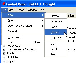
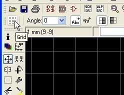
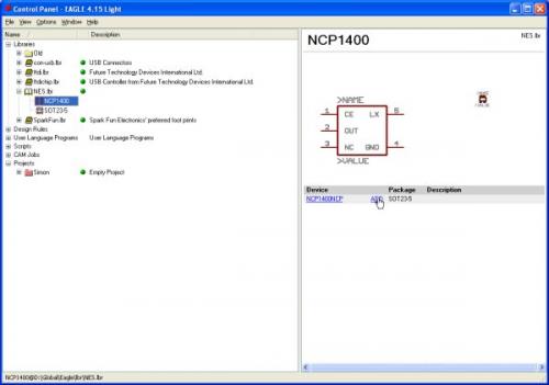
To start your first parts library:
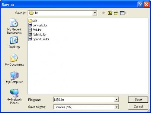
Once the Library Editor is open, hit the Save icon and save your library with your name on it:
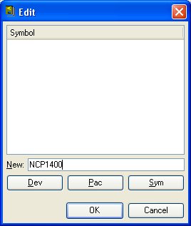
Click on create a new symbol. Name it 'NCP1400':
Create a red box by clicking on the 'Wire' button:
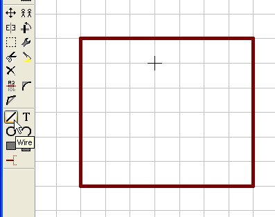
Don't worry about centering the box at this time.
Key commands to try out:
-
Scroll the scroll wheel on the mouse to zoom in/out
-
Click the scroll wheel (on the main work area) and hold shift to move the work area around
-
If the work area image looks corrupt, just zoom in/out to refresh the area
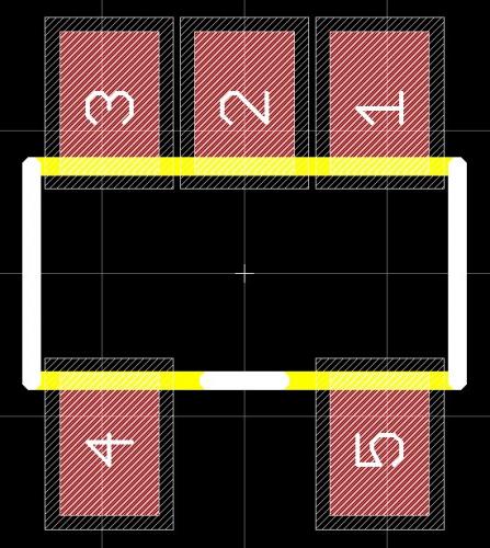
Add 5 pins to the box:
Press F4 and click on a pin. Name them according to the datasheet.
Pins are named, but we need to clean up how this part is sized and where the center is at. To grab the group press Alt+F7, click and hold, and drag from one corner of the work area to the opposite corner - boxing in the pins and part:
Once you have everything selected (everything should be highlighted red), press F7 and right click to move the group over the center cross. In my example part, I the right side was one block too far over so I sucked in the right side one square.

The image above shows the part centered and symmetrical.
-
NEVER change the grid size in the library editor or in the schematic layout editor. Leave it on 0.1inch steps and don't use the alternate 0.01 step. If you do, you won't be able to hook wires to the pin tie points.
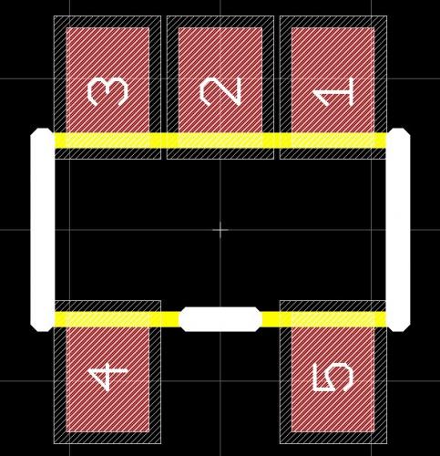
Name and Value tags are always nice. Click on the text button and type '>NAME' and '>VALUE'. (Ok I lied. It's okay to use the alternate step size when moving around non-critical items like text. Hold the Alt key down while your placing the Name and Value tags to get them where you want them):
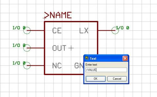
Once you have Name and Value placed, you'll notice that these are red when they are normally gray in color. Be sure to modify what layer these two strings are on. We need to change the >NAME tag to the Name layer, and >VALUE tag to the value layer. To do this:
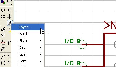
Click on the wrench, then Layer.. Choose the layer you'd like to change the object to

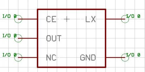
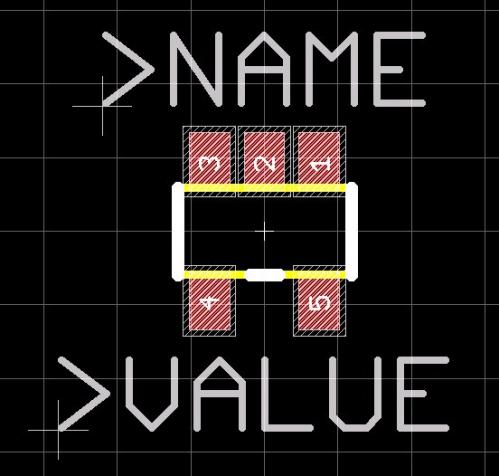
Here is the final schematic part, centered and happy. If you want, you can change the pin definitions to indicate which pins are inputs, outputs, pwr, etc. I find these settings useful in a handful of situations. This is a simple enough part, we'll skip it.
Now for the footprint. Remember, when in doubt create your own footprint. Trusting anyone else' footprint without scrutinizing it closely is a very bad idea. If you're lucky, your datasheet will include a recommended footprint for the part you are working with. If it does not, google for the words 'recommended land pattern SOT-23' or whatever package you are looking for. The words 'land pattern' is the key.
Lucky us! The NCP1400 datasheet has a recommend footprint:
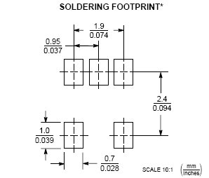
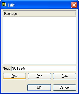
This takes some getting used to. There are two numbers from every dimension, and not all the dimensions are indicated?! Lower left corner shows mm/inches meaning the top number is the dimension in mm and the bottom number is that same dimension in inches. Sorry folks, it's a metric world. More and more devices are spec'd in mm only (connectors, ICs, etc). From the Library editor, click on Package and let's start creating the footprint for this device. This is actually a pretty common package type called SOT23-5, so let's use that name:
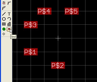
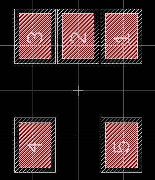
Throw down 5 pads:
Hmm, some of the layers are not showing - let's turn them all on:
Click 'All' and then 'Ok'. You should now be able to view the solder mask (in Eagle as the 'Top Stop' layer) and solder paste layers (aka 'Top Cream' layer).
Now back in your datasheet you will find the width of each pad to be 0.7mm and the height to be 1.0mm. Before we can go editing the pads, we need to put Eagle into metric mode. Press Alt+F10 and you should see the coordinates in the upper task bar switch to mm. To alter the size of the five pads to 0.7x1.0mm, click on the wrench, then Smd, then '...':
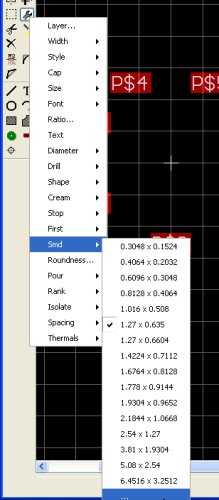
You will then be prompted to enter the X and Y dimensions in mm with an 'x' in between:
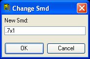
Remember the X dimension always comes first.
Now click on all 5 pads. All 5 pads should now be the correct size. I really prefer to center the footprint with the center of the work area. This means we need to work out the various dimensions:
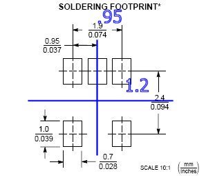
Let's start with the easy pad - pin #2 will be located at (0,1.2). Before we can start moving pads, we need to adjust the alternate grid so that we can get the the side pads to 0.95mm. Click on the points/grid box:
Change the Alt: box from 0.1 to 0.05 and click on ok. Now lets move pin 2. In the work area, press F7, then hold control and click on a pad:
F7 issues the move command. Holding control while clicking on a pad causes the pad to try to center to the cursor (this way you know that the coordinates displayed in the upper left task bar are displaying where the very center of the pad is at and not where your cursor may have been off when you first clicked on the pad). Because the pads are locked onto the 1mm grid, you'll notice the pad jump from 3mm to 4mm, etc. While holding control, hold alt as well. The pad should now jump on the alternate grid of 0.05mm instead of 1mm. Important buttons to know:
-
Again, the scroll wheel will zoom in/out
-
Clicking the scroll wheel will drag the work area around
-
Holding the shift key will allow you drag the work area further
To position this pad to (0,1.2) I literally had to:
-
Hold Control and click on the pad
-
Hold Alt, Shift, and control with one hand
-
Scroll in with the scroll wheel
-
Click+drag the scroll wheel to get the work area centered
-
Release Shift
-
Move the cursor to position (0,1.2) (Remember to hold alt!)
This sounds really scary but after creating two footprints, you'll have it down without thinking about it.
Nifty
Press F4 and click on each pad renaming them to match the datasheet numbering:
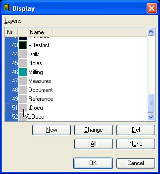
Did you number them wrong? Double check. Make sure you get it right! We need to add a dimensional layer to indicate the size of the device. This is different than a silkscreen indicator. I like to use layer 51 (named 'tDocu' meaning top document layer?). This layer will only be displayed while we're playing on the layout window and won't show up on any production files. This allows us to display the physical size of awkward parts, hopefully avoiding collisions between bulky parts when we go to populate the PCB.
Why should we even care about these layers?
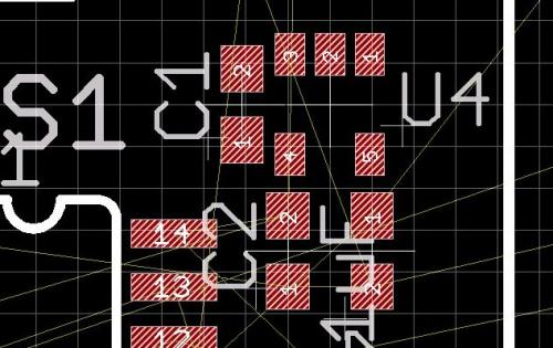
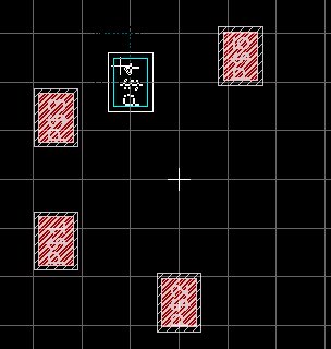
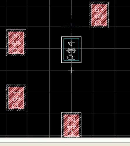
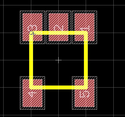
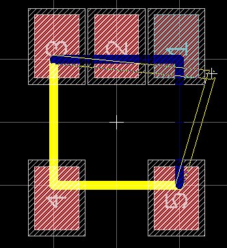
Here is our NCP1400 (label U4) next to three capacitors. See how crazy board layout can get? Notice C1 is next to U4 but the distance between them looks ok? When we add in the tDocu layer:
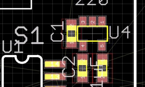
Whoa! That cap is way too close to the body of the NCP1400. You might be able to get those two components soldered onto the board, but it would be a mash up job. We need to know the rough physical outline of components during layout. To do that, we need to add a frame to our footprint.
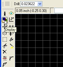
Before we add lines to our footprint to indicate the physical size of our part, let's change the layer color - gray is a horrible color to try to see! Click on the 'Display' button, scroll down to layer 51 and double click on the gray box next to 'tDocu':
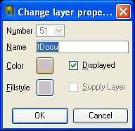
Then click on the gray 'Color' box and change it to something interesting like lemon yellow, then click ok. Anything you do on this layer will now be yellow.
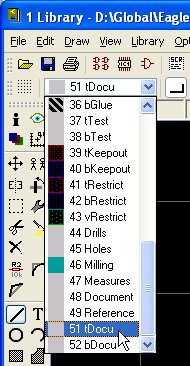
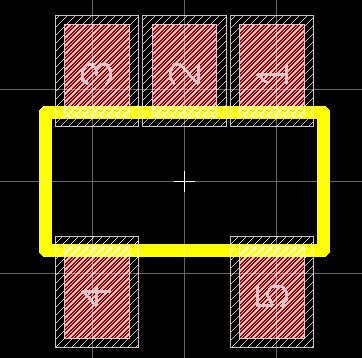
Click on the 'Wire' button. Select layer 51 (this layer will be yellow in the drop down box the next time you close/open the Library editor).
You should now be able to lay down yellow lines. Put four of them down in a box:
Press escape to stop drawing. Now we need to move the edges of the box to the outside edge of our part. Checking the datasheet again:
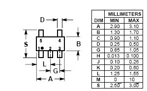
Ahh manufacturing tolerances. They can't really tell us how big the B and A dimensions will be, so I always pick a value in the middle of the min/max. A = 3mm, B = 1.5mm. Remember we have to center the frame so the upper right corner of the frame will be at (1.5, 0.75).
Now go back to the footprint, press F7 to issue the move command. Hold the control key and click on the upper right corner of the frame. When you do this, the 1 pad may light up - this is because Eagle does not know which part you are trying to move - the pad or the line? If you left click, Eagle will begin moving the 1 pad because it is highlighted. Right click and the frame should highlight. Now left click and you should be moving the upper right corner of the frame. I know, its really confusing at first. It's actually really handy once you're used to it!
Once you've got the corner at (1.5,0.75), left click to anchor the corner at that location and adjust the other three corners.
I can almost see it now! Notice how the part extends past the edges of the pads? If we would have put a component (like an 0603 resistor) next to pads 3 and 4 the two component may have been bumping into each other. Electrically, the layout would have been fine but when we would go to populate the PCB, this regulator might have been right up against the neighboring part.
Finally, I highly encourage you to add a bit of silkscreen to this part. What does a board look like without silkscreen?
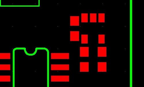
Can you tell where the components go and how they are supposed to get oriented without a silk indicator? I can't.

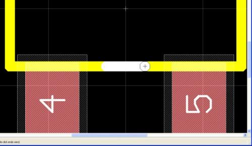
Add a little silkscreen and it's suddenly very apparent where the NCP1400 is supposed to go.
When you get a PCB with nothing but silver pads, the 4/5 pads on this part look a lot like the spot for an 0805 capacitor! Select layer 21 tPlace. You may notice this layer is gray as well! I hate gray. Re-color this layer to white. When you get your PCBs, the silkscreen is white, right? Might as well make them agree.
I zoomed way in, held alt to get onto the alternate grid, and ran the line from (-0.25, -0.75) to (0.25, -0.75). You really do not want to put silkscreen across your pads. This will negatively affect how the pads react to solder. It would foul a board or anything, it's just best to keep the silkscreen layer away from pads. You could butt the white line right up against the pad, but the silkscreen layers has the worst tolerances and the greatest skew. The white lines in your beautiful layout could end up a couple mm to the left or right when you get your PCBs from the fab house. Besides, 0.25 is such a nice start/finish number!
Create silkscreen lines for the sides as well. Don't worry about itty-bitty silkscreen lines inbetween the upper pads or the little corners. Very small silkscreen lines will either be ignored by the fab house or else they will just flake off.
When we laid out the tDocu layer, the wire thickness was 0.127mm or 0.005". 0.005" is also pronounced as '5 mil'. Time and time again, you will hear that fab houses can handle 8 mil traces and 8 mil spacing for their basic service (aka their cheap service). This means that no trace can be less than 0.008" in thickness and two traces cannot be closer than 0.008" to each other. Well guess what thickness our silkscreen traces are? The 5mil tDocu lines don't matter because they will not be printed or fabbed, but the 5mil silkscreen traces may give some fab houses fits! The fab house may increase the line thickness to 8mil, they may try to print the 5mil line as is and have it come out very thin with no weight, or they may not print it at all! Let's alter the thickness of the silkscreen lines to 8mil so that we are kosher with any fab house.
We're switching back to Imperial units! Press F10. Next click on the wrench, width, and '...':
Why doesn't Eagle have 8mil listed? I have no idea. Enter 0.008 into the box prompt. Click on the three silkscreen lines:
It looks a bit odd, but once you see it on a PCB, it will look great! The last things we need to do (I promise!) is to add a >NAME and >VALUE tag. Review the schematic component section to see how to do this in detail. Add two strings ('>NAME' and '>VALUE') and then modify the layers for these two strings to tName and tValue respectively.
And we're done with the footprint creation for this one part! Now you see why engineers and companies hoard their libraries. The first couple footprints you create will be totally botched and will probably kill your PCB layout. But once you get a part created, and you use it once or twice successfully, the part will be proven and you'll never have to worry about it again! With a collection of 20-30 known good parts, you'll be able to whip up very reliable PCBs in surprisingly little time.
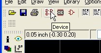
To finish this part in our library, we need to relate the pin numbers on our footprint to the pin identifiers on our schematic part. Save your library and click on the Device button:
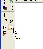
Name the new device NCP1400 and then click on the Add button:
Drop the schematic part in the center of the work area. Hit escape twice to get rid of the part window. Now click on the 'New' button in the Package area:
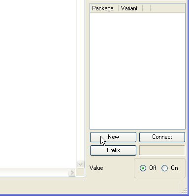
Double click on the SOT23-5 listing.
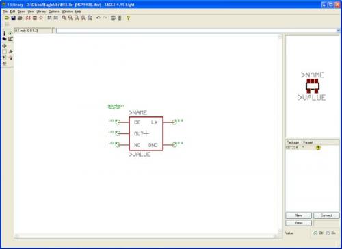
Notice the yellow exclamation point in the Package area? This means that a footprint is associated with the schematic part but the pins have not yet been assigned. Double click on the 'SOT23-5' text in the Package area:

Review page 1 of the NCP1400 datasheet to know what pins connect to what pad numbers:
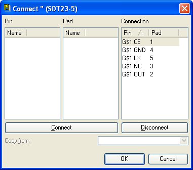
Double clicking on a given name on one side will assign it to the highlighted choice on the opposite side. You've done a great job up to this point! Double check that your pad assignments are correct!
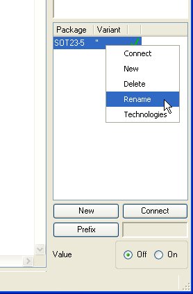
Right click on the Package name and click on Rename. Various different footprints can be associated with any given schematic part. To differentiate between parts, you can give the pin assignments different names. I mis-use this function a bit. I often name variants 'SMD', 'A', 'B', '8', '10', or in this case 'NCP1400'. Pick your poison.
It's ok if you do not give this device a variant name, but if you leave the default variant name as " and then try to add a new pad assignment you will get the "Package variant " already defined!" error:
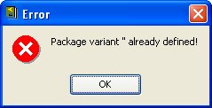
Just rename one of the variants to a different name so that Eagle can add this new variant with the default " name.
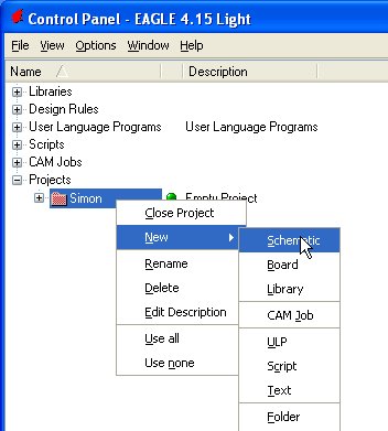
Now let's add this newly created part to our schematic. Close the library editor and go back to the Eagle Control Panel. Click on File->New->Project. Name this new project - in this example we'll do 'Simon'. Right click on the Simon project and create a new Schematic:
The schematic editor should open. Now go back to the Eagle Control Panel and open your new Library:
You should see the NCP1400 part and the SOT23-5 footprint. Highlight the NCP1400 part and in the right screen click on ADD. The schematic editor will pop up allowing you to place the NCP1400.
And that's it! You now know how to create a component from scratch. Be sure to do a 1 to 1 print of your layout before sending it to the PCB fab house to verify all the parts against their respective footprints.
Lecture 1 - Background and Power Supply
Lecture 2 - How to Get Code Onto a Microcontroller
Lecture 3 - What is an oscillator?
Lecture 4 - UART and Serial Communication
Lecture 5 - AVR GCC Compiling
Lecture 6 - Soldering Basics
Lecture 7 - SMD Soldering
Lecture 8 - Eagle: Schematics
Lecture 9 - Eagle: PCB Layout
Lecture 10 - Eagle: Creating a new part
Common Mistakes, Tips and Tricks
Great tutorial, but I think that the procedure outlined here for accurately sizing and positioning SMD pads is way more complicated than it needs to be. I've found that there's really no need to mess with multiple grid spacings or complicated shift key combinations. Simply:
1) Click the SMD button and enter the size of the pad you want (0.028 x 0.039 in this case) into the field at the top of the window
2) Drop the five pads by clicking once for each
3) Here's the fun part -- click the info button, then sequentially click on each pad and set the X and Y coordinates per the data sheet. These coordinates are especially easy to calculate when the origin is set to the middle of the package, as was shown in this tutorial. The coordinate pairs are simply:
Pin 1 (-0.037,-0.047)
Pin 2 (0,-0.047)
Pin 3 (0.037,-0.047)
Pin 4 (0.037,0.047)
Pin 5 (-0.037,0.047)
Note that I laid out my package with Pin 1 on the lower left, so the coordinates shown will reflect that.
I hope this will help other would-be EAGLE part creators like me. Thanks, SparkFun, for creating these great tutorials, and for recommending EAGLE!
Cheers.
You really should update these to the latest version of Eagle, curently 5.2.0. The shortcut keys don't match up and the screen shots are all different.
But nice job, thanks!!
Thanks for this very helpful tutorial. My only suggestion is to please add the note: if your SMD pads have no visible names, you need to type magic incantation: "set pad_names on"
I hadn't read the comments here, so I discovered this thanks to Oliver Betz in the user forum (a newsgroup- remember those?) news://news.cadsoft.de/eagle.userchat.eng
Some forums also at http://www.eaglecentral.ca/forums/
When I got to this part:
" To finish this part in our library, we need to relate the pin numbers on our footprint to the pin identifiers on our schematic part. Save your library and click on the Device button: Name the new device NCP1400 and then click on the Add button:"
All the work I did got completely erased!!!!!!!!!!!!!!!!!!!!!!!!!! I'm using Eagle 7.2.0 by the way and it's not the same as what you are describing.
HELP PLEASE!!!!!!!!!!!!
Any work you did in the symbol or package design sections should still be there )(short of the program having crashed). The 'Device' section just changes the view to one where you can add packages and symbols together, but it doesn't automatically add the last package and/or symbol you worked on. Have you pressed the symbol/package button (or menu: Library, Package / Symbol), and looked for your part(s) there?
thanks so much, for this tutorial. very helpful...
I think it would be very helpful to show some photos of the finished part if it was ever made.
Thank you, that was a nice introduction.
Thank you SFE!!!!
Guys, thanks so much for the time and effort you put in writing this tutorial. I learned a lot. I created my first SMD part: a MicroFET for Fairchild Semi #FDFMA2P857. Really, thank you!
both worked like a charm! thanks Mike.
Is there also a way to name multiple pins the same name? I have two no-connects on my MCU right now and it won't let me have two N/C's. Thanks.
Try naming them e.g. NC@1, NC@2, etc. This is a trick like the overbar; it shouldn't display anything after the '@'.
Hello Mike this tip solved one of my big issue for naming multiple pins. One more thing I would like to know how to avoid "$" from naming part on schematics and boards for components ? e.g. 'U$1' should appear as 'U1'. I checked your eagle rules for sparkfun, it is clearly mentioned to fix it, but not inform how to do it. Thanks
Thanks for the tutorial! I just found that delimiting BOTH ends of what you want to show as negated with an exclamation mark (!) communicates where to end the overbar, ie GP3/!MCLR!/VPP.
Is there any way to get rid of those annoying green circles on the pins? I'm having trouble finding a way to remove them.
If you turn off the "pins" layer in the schematic, you won't see the green circles.
Great tutorial, it works almost perfectly. My only problem was with putting the >VALUE label on. When I try to modify the value of the part in a schematic, a prompt pops up saying "Part 'X' has no user definable value. Do you want to change it anyway?"
I can then change the value, but it's really frustrating having to hit ok on this prompt for every single component in the project. Do you have any idea what might be causing this?
please fix the pictures, i cant see, i want to learn
As joshie mentioned on the page for Lecture #8, some JS code will fix the images temporarily (until you refresh the page).
The pictures here on this page are all broken.
I'm really looking forward to viewing this tutorial.
No images!!!
I cant see any image :/
Hi!!! This is a great tutorial but I'm trying to make a part for the Sparkfun XBee Breakout Board (since I want the XBee to be removable from the board). It's clearly not a surface mount so I was wondering if anyone could give me some tips on how to go about manipulating this tutorial for my part (I'm really new to Eagle).
Great tutorial. Just I want to add that when naming the I/O(Inputs/Outputs) in the Symbol section, you can add an exclamation mark "!" before introducing the name of the I/O if Pin is negated. Like Chip select -> (!CS). And a line over the name will appear magicaly.
::@
=D
Helpful tutorial, I'd just like to request a section for making footprints for through-hole parts like DIP ICs.
Also, you can verify your part's layout by making a board with just that part on it and printing it out, instead of having to guess and check on PCBs.
Great tutorial but a quick question. I have some parts I always use in the same way (caps at certain pins, etc.). Is it possible to enter pads and connections for multiple parts to form subcircuits that can be placed all once?
In part layout, I fooled with the ctrl alt shift move business, its to painful (bad wrists). Just use the command line.
name the pin
then type
move pinname (x y)
for example
move A1 (1.23 2.44)
no fuss and its exact
Thanks for the tutorial!
I have question about changing IC soldering pad dimension. When i print layouts trough laser printer, there is no space between pads and on error check i have clearance issue on these pads... I use pcb and schematic from sparkfun Aruino Mega and Ardupilot Mega. Eagle is configured as written in one of SparkFun tutorial(*.Cam, *.drm ) Also if i ripup original pcb and do autorouter.
Thanks in advance,
D.
When creating a footprint and throwing down the pads in the Layout Editor the pin names are not visible (even when all the layers are turned on).
How do I enable the display of pin named in the Layout Editor?
"set pad on" and "set pad off" in the command line
Losing my mind... Cant figure out how to turn off or delete cream and top stop from a pad. I need the pad to be covered with silkscreen... so no paste over it either.
Awesome, I helped a local engineer with his project and now he is going to patten it and asked me to lay out his boards. This is exactly what I was looking for to bridge the gap between beloved express pcb and industry standards. These tutorials are an incredible wealth of useful knowledge and I too recommend updating them. Time to make a few of my boards so any mistakes can be discovered privately.
Excellent tutorial! Thanks!
When you talk about 8mil stuff for the silkscreen, and it being 0.008" Do you not in fact mean 8thou? I'm no EE, I'm in mech eng, but when I talk to the machinists about something that's 0.005" for example, I would say "5 thou"
Great tutorial, thanks!
Mil is a unit just like thou and 1 mil equals to 0.001 inch. It's also referred to as "point". So you are also correct in calling 0.008" as 8 thou. I think both mil and thou comes from mixing the metric system with the English system. Thou probably comes from "thousand" and Mil probably comes from "milli". In CAD or PCB layout program, you often work with Mil rather than Thou.
Mil is an abbreviation of "milli-inch" so there's no contradiction here - "thou" is just a shorthand jargon. They're all thousands of inches.
In fact in Eagle 5.7, if you go to "Grid ..." option under "View", you can set the units and your choices are mic, mm, inch, and mil.
Thank you, Thank you very much for sharing.
I learned about PCB Layout in 3 days from your tutorial.
Excellent Job, Thanks.
Thanks a million for this, it's the best tutorial on the subject that I've been able to find.
I must say, tho, that time and time again everybody in the Eagle world warns against the sharing of libraries, and insists that hoarding your own is the only safe bet. Then in the same breath, they explain that you're going to waste a huge amount of time and money screwing up your own libraries until you learn to get it right.
This is dumb. Sharing is good! Why should everybody need to reinvent their wheels? A reliable, trustworthy open-source repository of Eagle libraries, guaranteed to some specification of quality, would be of immense benefit to every single user of this software. It really obviously needs to exist, and yet I can't find it. Am I missing something obvious? Why is nobody doing this? It's madness. Nobody in the software engineering world would tolerate such a vacuum around such a crucial toolset.
SparkFun is in a good position to spearhead such a project. You already distribute a good library. How many people do you think are using it?