
Sizing a heat sink for a heavy load
Heat sinks and thermal dissipation
In a previous tutorial, we discussed the need for a heat sink in situations where a device is expected to dissipate a large amount of heat. But how much heat sinking is needed? When do you need a modest folded metal heat sink versus a whopping milled-out-of-aluminum heat sink versus a mondo great fins-and-fan heat sink?
If you’re like me, at first glance, this problem seems intractable and you really start wishing you’d taken that thermodynamics course in college. But fear not! It’s not as bad as all that. Most datasheets will tell you what you need to know to come up with a rough estimate (accurate to within perhaps 50%) of how much heat sinking you really need for your application.
The problem defined
As an example, I’m going to use a circuit that I’ve developed for another tutorial I’m working on- a digital constant current load for discharging batteries so I can characterize their power capacity. The core of the load is an RFP30N06LE N-channel MOSFET. I’m not going to get into the circuit design required to use that as a constant current load here- if you’re really interested you can flip over to the digital load tutorial for more details.
At any rate, for this application, I’ve set my goal as being able to discharge a two-cell LiPo battery at up to 2A constantly. Freshly charged, that two-cell battery will be at approximately 8.4V, which means I’m setting myself up to dump 16.8W (P = I*V where I = 2A and V = 16.8V) into my FET. Note that this is worst case- that 8.4V is going to drop fast as the battery discharges, and if I’m NOT using a two-cell battery, the load will be even less.
Let’s do a little derating, too- if our worst case is 16.8W, if we target, say, 30W, then surely we’ll be in the clear- that’s almost a 100% slop factor.
Collecting the necessary information
Remember how I said most datasheets would tell you what you need to know to solve this problem? Let’s paw through the RFP30N06LE datasheet and the milled aluminum heat sink datasheet and see what we can come up with.
Fortunately, device manufacturers know that the datasheet target audience is people who are familiar with Ohm’s law. The information we need is described in terms of ºC/W and is referred to as “thermal resistance” (hereafter "Rt"). In the RFP30N06LE datasheet it’s at the bottom of the second page, in the “Electrical Specifications” section:

Note that there are TWO values here- one for “Junction to Case” and one for “Junction to Ambient”. We can basically ignore the “Junction to Ambient” value: that’s information for the device when there’s no heat sink in place. The "Junction to Case" value is the thermal resistance between the actual semiconductor die inside the plastic and the big fat metal tab hanging off the back. This is the critical value- if TJ gets too high, the device will fail.
In the heat sink datasheet, there’s a value given in a box on the second page:
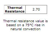
In other words, for this heat sink, with no fans or forced air or other cooling shenanigans (“natural convection”), we can expect the temperature of the heat sink to rise 2.70°C above ambient for every watt it’s trying to dissipate.
Thermal circuits
How does this relate to Ohm’s law? Well, if we can write Ohm’s law as
R = V/I
then, based on the units of thermal resistance (°C/W), we can write the thermal resistance version of Ohm’s law as
Rt = T/P
What does that mean, in practical terms? It means that you can draw a thermal circuit where thermal resistances are equivalent to resistance, temperature is equivalent to voltage and power dissipation is equivalent to current.
Confused yet? Let’s take it step by step.
Doing the math
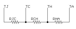
Let’s start by drawing out a circuit diagram of our system, with voltages replaced by temperatures and resistances replaced by thermal resistances:
where
-
TJ is the temperature of the semiconductor junction
-
RJC is the thermal resistance between the junction and the case (1.55°C/W as given in the datasheet)
-
TC is the temperature at the surface of the package
-
RCH is the thermal resistance between the case and the heat sink (.25°C/W; see below)
-
TH is the temperautre at the surface of the heat sink
-
RHA is the thermal resistance between the heat sink and the ambient air (2.70°C/W as given in the datasheet)
-
TA is the ambient temperature (25° is a pretty standard value for room temp, but this can go up if your device is in an enclosure or a more trying environment, such as outside in the sun)
-
P is the power from which we are attempting to dissipate heat (30W)
RCH is going to vary depending on what method you use to join the case and the heat sink. If you just screw them together, it won’t be very good- perhaps as high as several °C/W. With a little dab of thermal grease, however, you may be able to safely ignore RCH. For our example, I’m using a conservative value based on values I’ve seen in a few white papers on the topic.
So, now what? What’s our goal, here? Well, we need to calculate TJ based on the power dissipation of the circuit (30W) and decide whether TJ is a safe value. If this were an electrical circuit, we could simply add up the resistances and multiply those by the current to find out what the total voltage across the three resistors is:
V = I(R1+R2+R3)
In a thermal circuit, Rt is analogous to R, T is analogous to V, and P is analogous to I. Therefore, we can write:
TJ = P(RJC+RCH+RHA) +TA =30(1.55+.25+2.7)+25 =160°C
Ouch! That’s hot! But, is it safe for the device? Let’s refer to the datasheet. On page two there’s a section labeled “Absolute Maximum Ratings”, which provides a maximum operating temperature of 175°C. Well, we aren’t violating the datasheet maximum value, but there’s not a lot of overhead to spare. Remember, though, that we built in almost 100% slop factor on our power dissipation. If we re-run the calculation with our ACTUAL intended power dissipation of 16.8W, we’ll get a temperature just above 100°C- hot enough to boil water (or burn your finger badly) but quite a ways below our datasheet maximum.
What about the heat sink? How hot will it be, here? After all, it's this big honking thing sticking out into space right where you're very possibly going to touch it- how bad a thing is that going to be? Well, that's simply a matter of taking the power (16.8W) times the thermal resistance of the heat sink (2.7°C/W) and adding that to the ambient temperature (25°C). That tells us that the heat sink, at 16.8W, will rise to about 70°C- about 160°F. Too hot to hold, but probably not instantly skin blistering.
The next steps
What if I hadn’t been happy with the answer? How could I improve matters?
Well, looking back at our system equation, the parameters that we can control to some degree are TA (running it in a cooler room or using a Peltier cooler perhaps), RHA (use a better heat sink, or forced air cooling) and RCH (use a better grade of thermal paste).
We could also try to reduce the power dissipation by, say, using multiple loads in parallel to share the power dissipation and decrease the temperature rise of each one. In fact, for the actual circuit, I elected to do just that- placing two MOSFETs in parallel to reduce the temperature dissipation of each one. For more on that, see the digital load tutorial.
Does anyone know where the 'digital load tutorial ' is ? The link above is bad... cheers
I know this is an OLD article, but just came across it...Lots of good info.. Just one minor typo found: "two-cell battery will be at approximately 8.4V, which means I’m setting myself up to dump 16.8W (P = I*V where I = 2A and V = 16.8V) "
Outside of that, I learned a few things today..Thanks for the write up!
In the " Sizing a heat sink for a heavy load " tutorial, you reference another tutorial: "digital load tutorial ", but the link to it is broken. Can you point me to it, or email me a copy please? I'm interested in the information on paralleling 2 MOSFETS, which is covered in that tutorial. Thanks, Doug
This is a very detailed article but I think it still might be a little confusing for newbies. I've created a more succinct guide for selecting the proper heat sink here: http://engineerdog.com/2014/09/09/free-resource-heat-sink-design-made-easy-with-one-equation/
You use the 2.7 C/W value from the datasheet, however, these calculations are slightly different than the one in the aavid.com site (http://www.aavid.com/sites/default/files/literature/Aavid-Board-Level-Heatsinks-Catalog.pdf#page=10).
Also, the chart on https://www.sparkfun.com/datasheets/Prototyping/General/PRT-09576-6400BG.pdf is a bit confusing; the arrows refer to both the curves.
In looking at some curves, the value seems to be OK, as the devices are linear:
The smaller 507302B00000G - thermal resistance is 24, on the graph, 5W is about a 100 C rise (20 C/W, roughly)
The 6400 BG - thermal resistance is 2.7, on the graph, 20 W is about a 65 C rise (3.25 C/W, roughly)
The 530001B02500G - thermal resistance is 8.0, on the graph, 20 W is again a 65 C rise (3.25 C/W, roughly), but the curve is non-linear; the 8.0 value seems a bit large too. Note that the 530002B02500G has a thermal resistance of 2.60, but the same graph! Maybe there was an error on the Aavid site?
Any thoughts on this, or am I missing the obvious?
Newbe question: When I'm looking at a device's datasheet how do I find the: "maximum current draw"? For example when I'm looking at my MCU datasheet it says "Max current sourced by ports: 200mA, Max current sunk by ports: 200mA, Max output current sunk/sourced by I/O pin: 25mA,etc" Should I select the 200mA or add both the sourced & sunk or do I add up all the i/o pins (25mA) that are currently in use? I want to clearly understand how much current to use in the power equation. Thank you in advance!
That means that ALL your I/O ports, together, can source/sink up to 200mA. Each individual pin can only source/sink up to 25mA. In other words, you could have eight pins do 25mA, and your MCU would be doing 200mA. You could also have ten pins do 20mA and have a total of 200mA. What you can't do is, say, have four pins draw 50mA for a total of 200mA (too much per pin) or have ten pins draw 25mA for a total of 250mA (too much total). To answer your question directly, your I/O ports will draw up to a maximum of 200mA (plus any losses to heat in the chip).