
Pseudo-Datasheet for the Serial ADXL
We have created a monster. The serial ADXL started out as a simple project that quickly ballooned into all sorts of madness. We have decided to post this project (as well as several others), all completely wide open, in an attempt to redeem ourselves. Read this stuff and take it to heart - it may save you from ripping out your hair on a project of your own.
The following info corresponds to the Serial ADXL breakout board offered on the main SparkFun.com website.
Navigate:
Intro - PCB woes and where stuff goes
Firmware - The current firmware implementation
PCB Revision 3 - SADXL - The Next Generation
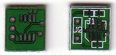
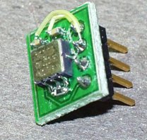
Serial ADXL PCB - revision 1
So what is this serial ADXL?
It was a simple plan - take a tiny PIC (SOIC 12F629), an Analog Devices ADXL202E, and some firmware, and make a little board that reads acceleration in the X and Y axis and outputs that info serially. Everyone loves a good 9600bps signal.
Why didn't anyone tell us?!
Our first PCB for the 202E worked ok, except for one mistake on our part - we forgot to read the data sheet!
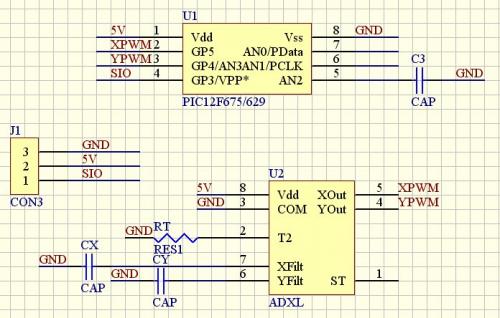
First Revision Schematic
What's wrong with this picture? GP3 (Pin 4) is in charge of outputting the Serial signal. But if you read the Microchip datasheet for the 12F629/675 section 3 you should see something like this:
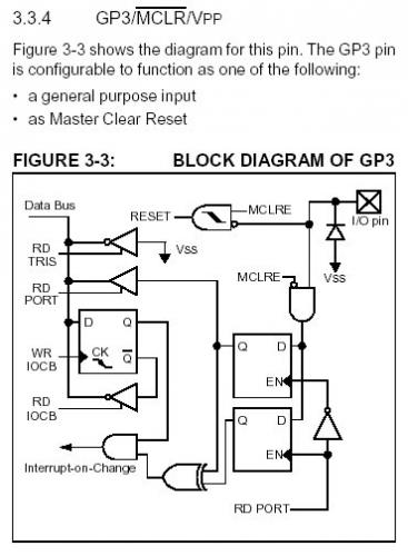
General purpose Input. No output capabilities. So with a little 30awg wire jumper, and some PCB scraping, we fixed AN1 (Pin 6) to be the output man. Ugly, but it worked.
Low cost? Yes please!
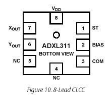
Then we stumbled upon the ADXL311. It stuck out on the www.analog.com website as being the "Low-Cost" ADXL. Anything is better than paying $12 each for the ADXL202E. What does low-cost mean? The ADXL311 outputs an analog signal rather than a fancy PWM signal.
An analog signal may sound scary at first, but you forget! The 12F675 is the 12F629 except with a 4-channel A/D converter. Oh boy! So we scurried off and quickly laid out the second revision serial PCB:
Ok, what's wrong with this one?
Again, we are idiots. We failed to read the ADXL311 datasheet thoroughly enough to get to the Pin-out diagram.
Doh!
There seems to be a few 'NC' (no connection) pins on this version. Pin 4 and 5 that were the X and Y PWM output signal pins are now NC? That's because the ADXL311's analog signals come out of Xout and Yout (Pin 7 and 6). So we managed to create another PCB with fouled wiring.
It works - just not like it was supposed to.
Is it broken? Not really. The SIO problem was fixed (moved to Pin 2) so that was ok, and we added C1, a decoupling capacitor for a cleaner power supply. And as long as we continue to use the ADXL202E on this board, everything is peachy. So the Serial ADXL r2 works great with the 202E. We also cleaned up the silkscreen a bit.
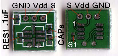
Serial ADXL - revision 2
Here is the info you need to know for the 2nd revision. From the silkscreen side, Ground is the first pin, followed by Vdd, and the serial signal. The bias resistor is the loan pads next to the ADXL. The CAPs are located next to each other. And there is a decoupling capacitor (.1uF - nice to have, but not critically required) located in the corner.
On the flip side, Pin 1 of the 12F675 (we are shipping the board with the 12F675 with A/D, but you can also use the 12F629 on your own until the 3rd revision) is located towards the 3-pin header. See how Pin 1 of the PIC is connected to Vdd? That's a good thing.
S1 is a control jumper. This is not really incorporated into the firmware yet, but we like to put it on there for future firmware revisions (PCB revisions, firmware revisions, yea!). In theory, you will simply solder the two pads together effectively pulling that pin to ground. This is read by the firmware as an 'Option' switch and the appropriate routine is run. For example, true 9600 baud output verse bit-banged RS-232 output. But again, there ain't nothin there in the firmware, so just leave these pads alone for now.
I forget where I stumbled upon Beerware, but I really like the idea. Yea, GNU is fun and all, but too many words, too many ideological camps. So here's the deal. If you like this code, you are welcome to use it. But if we meet someday, you buy the beer.
Let this page serve as a datasheet of sorts for the output of the Serial ADXL.
It took me a few searches on Goggle before I found the originator of Beer-ware. Gotta love the Danes.
http://people.freebsd.org/~phk/
/*
* ----------------------------------------------------------------------------
* "THE BEER-WARE LICENSE" (Revision 42):
*
* can do whatever you want with this stuff. If we meet some day, and you think
* this stuff is worth it, you can buy me a beer in return. Nathan Seidle
* ----------------------------------------------------------------------------
*
*/
Navigate:
Intro - PCB woes and where stuff goes
Firmware - The current firmware implementation
PCB Revision 3 - SADXL - The Next Generation
Oh yea - get the current firmware:
sadxl - c asm hex - The main firmware program or the 12F675
soft232 - c - The supporting routines for software based 9600 baud signal generation
s-test - c asm hex - A test routine for the 16F873A. Looks for the 0xAA and 0xDA start/stop bytes and outputs the incoming data stream.
What's it do?
The Serial ADXL firmware (yes, it can be pronounced sad-ixl) takes the PWM signals coming off the ADXL202 as counter values and sends them down the line in a conversation. This is a made-up word for a series of bytes.
The conversation looks like this:
Start byte -- Data Byte1 -- Data Byte2 -- End Byte
0xAA -- 0x?? -- 0x?? -- 0xDA
The Start byte is always 0xAA, the End Byte is always 0xDA. The program you write for the microcontroller of your choice should look for the start byte and begin to record. It should then verify that the fourth byte received is the terminator byte 0xDA. If it is not, then trash it - you just read some funky noise. Take a look at s-test.c for an example of how we implemented this on a 16F873A.
Open up sadxl.c and look at the main loop:
//Get 10 readings in the X direction
for(x = 0 ; x < 10 ; x++)
{cx = 0;
while(XPWM == 1); //Wait for current Pulse to end
while(XPWM == 0);
while(XPWM == 1) cx++;
counter_x += cx;}
This loop finds one PWM signal and counts how long it is. It does this 10 times and then divides by 10 to get the average. This loop should nominally take 10-20ms to execute depending on your timing resistor value (RES1).
The code then does the same for the Y direction. It then outputs the 4 byte array.
//Send out the data array
for(x = 0 ; x < 4 ; x++)soft_rs_out(data_array[x]);
Pretty simple stuff. The Serial ADXL is pretty dumb, but it serves it's purpose. The output bytes are really only the counter values from the X and Y loops. These are important because you simply hook up the Serial ADXL and take a look at what counter values it is outputting. Let's say at rest the board is sending out data bytes 0x83 and 0x86. Now when you tilt the board on one axis, the second byte increases to 0xA5 until you reach vertical. If you know what you are doing, you can make a pretty decent tilt sensor out of this thing. But because the counter values do not become too large, we can also use the serial board as a dynamic sensor - ergo, we can shake the board around and watch the counter values go crazy as the accelerations go crazy.
Oh, and if you've read this far (wow) - here is something to checkout:
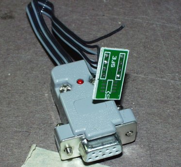
SOIC Programmer
It's our home-made SOIC programmer! Using a butchered PG1 (I forget why it was cut), we wired the appropriate control lines to the lines on the 8-Pin SOIC to DIP adapter PCB. For production programming, we simply line up to SOIC 8-Pin PIC to the pads on the PCB and squeeze it there while we run ICProg to get the firmware onto the PIC. After programming is complete, we run a read/verify to make sure it worked, and it's off to the Serial ADXL board to be soldered on!
We still need to fix the problem with the ADXL303 vs ADXL202E. Not a huge deal. But is it?
Navigate:
Intro - PCB woes and where stuff goes
Firmware - The current firmware implementation
PCB Revision 3 - SADXL - The Next Generation
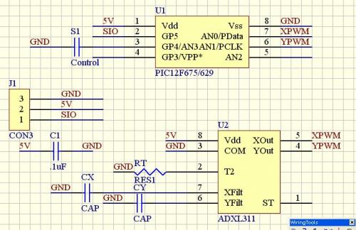
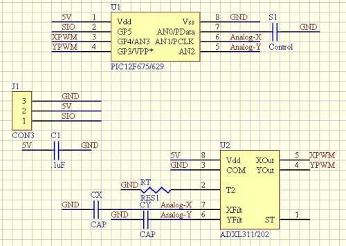
Here is the schematic for the 3rd revision using the 12F675 A/D converter:
Yea - more magic with the wires!
We've fixed a lot with this one. The PWM signals are still read so the 3rd revision will continue to work with the ADXL202E. The analog signals from the ADXL311 will be read be separate pins so the 3rd revision PCB will also work with the cheaper ADXL311. And lastly, the control jumper is attached to a pin that has a weak internal pull-up resistor. Cool, huh? Let's hope it works in practice.
Tests with the ADXL311 -
Ehh, you get the idea
We've hooked up the ADXL311 to one of our Tiny ADXL breakout boards. Do not try this at home unless you understand the issues concerning the difference between the ADXL202 and ADXL311. It took us two tries - and we designed the thing! We had to cut the traces connecting XPWM and YPWM pins. And then jumper the Xout and Yout pins of the ADXL311 (shown in the picture as the input side of the filtering capacitors) to the XPWM and YPWM pins. Ugly, but it works.
So you've got an analog output signal coming off the ADXL311, now what? We attached the Xout and Yout signals to the A/D converter on a 16F873A. Take a look at the ADXL311 datasheet. Can ANYONE find where it references what the analog signals look like? Maybe I am missing it, but I've read that thing numerous times and cannot determine from the datasheet how the level of the analog signal corresponds to the acceleration. Yes, Analog Devices, it's proportional, but by how much!?
They give us a hint under "Using the ADXL311 with Operating voltages other than 3 V". "At 5V the output sensitivity is typically 312mV/g." Really? Thanks guys. Do they mention ANYWHERE what the relationship is between the analog voltage level and the measured gravity? Nope! Grr.
This means that at a full tilt (+1 gravity), the signal will increase by 312mV. If the original signal (at level) is at roughly 2.5V, we should read 2.812V off the ADXL311. Similarly, 2.188V will be read at -1 gravity.
Does not play well with numbers -
The ADXL311 is good, but with an output signal change of only +-312mV for 180 degrees of tilt, things are going to get dicey.
The 12F675 has a 10bit A/D converter. That's 0x000 representing 0V and 0x3FF representing Vdd (or 5V in our case). A little math:
0x3FF is 1024 decimal so 5V / 1024 bits = 4.88mV per bit change
The A/D converter can roughly detect a change in 4.88mV. Jeesh! Way to go MicroChip. We have 312mV/gravity sensitivity. This is seen by the A/D converter as:
? / 2.188V = 1024 / 5V
? = 448 - This is the decimal value produced by the A/D when the ADXL311 detects -1g.
? / 2.812V = 1024 / 5V
? = 576 - This is the decimal value produced by the A/D when the ADXL311 detects +1g.
576 - 448 = 128
There is a change of 128 from 0 to 180 degrees.
180 degrees / 128 = 1.41 degrees per bit change
This is the big problem. The Serial ADXL with the ADXL311 will be able to detect a change in 1.41 degrees of tilt in optimal circumstances. It's probably going to be more like 5-10 degrees with temperature and noise errors.
Ahh, so that's why there are signal amplifiers on all the ADXL311 eval boards from other vendors. With a double or quadruple signal amp, the resolution gets lots better. We build 'em small, and dirty. Use the Serial ADXL for experimentation and fun, but know that you won't be controlling your autonomous aircraft with it.
Take me back to the intro
Comments 0 comments