
SMD How To - 5
What do I do when...?
You are going to lift pads. Sometimes, there is nothing you can do to prevent it. If a pad is lifted, and you have access to the design files, you can usually find out where the pad was supposed to be connected to. In the case of this example, you can simply see a trace running from where the pad used to be, and where it connects to a via. Since the pad is now gone, you can jumper from the via directly to the pin on the IC, thus re-creating the electrical connection.
This is called 'green' wiring because historically, assembly houses used green wires to try to make it blend in with the board. Any kind of 'green' wiring is considered poor design on a commercial product, but is completely acceptable for saving protos!

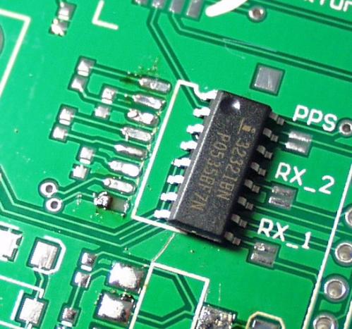
Poor poor pad

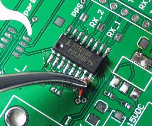
Solder the IC down as it should be, but forget soldering the pin without the pad

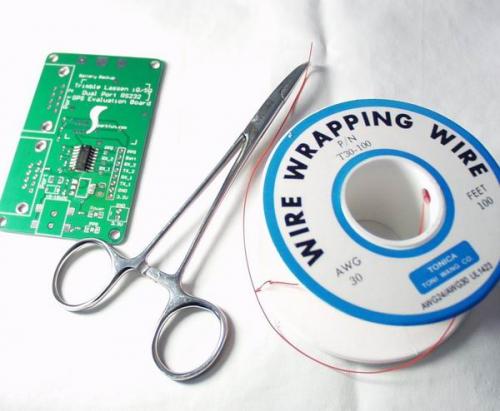
Here is the 30AWG wire wrap wire and the very necessary hemostats.

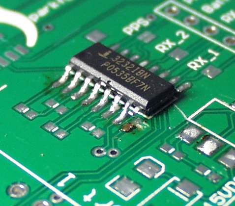
Here is what I call 'wing-ing' the pin. This is also a good method when the pad is available but goes to the wrong place. Because of schematic errors, if the pad goes to the wrong place, just wing the pin and solder a jumper from the winged pin to the correct place on your PCB.

Measure the correct length of wire. No point in making the jumper 2" if you only need 0.2". Use 30AWG wire strippers or adjustable wire strippers (set to a small aperture) to strip the jumper. You'll notice I strip very little from the ends on the wire. This helps prevent jumpers from local pins to the exposed jumper wire.
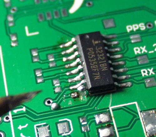

Dome the via and pin where the wire is to attach.
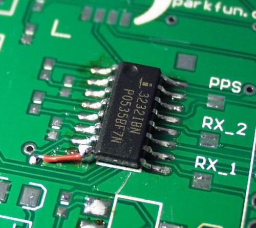

And solder 'er down. The PCB is saved!
This green wire method is used for all sorts of errors. We often have to cut traces with the exacto knife and then green wire jumper. Get creative. I highly recommend working every bug out of a layout before running a revision. Even if it's ugly. It's really bad practice to find one layout bug, quickly re-run a PCB with the correction, and then find out there are a whole handful of other errors.
This is one of my favorite images from our history museum. This board was completely messed up. But with a significant amount of work, we got the board functioning. By doing so, the next board revision worked! Had we not found all the trace problems, it would have taken many more revisions. Always trouble shoot every function and feature of a design before settling down to revise a board.
Page 6 - Sneaky tricks for soldering leadless ICs
There seema to be quite a few images missing from the article.
might mention that with cmos, mosfet, fet electronics solder suckers have been implicated with esd (electrostatic discharge) damage. So solder wick is preferred for these items, ive heard.
Some great tutorials I've been reading. I repair industrial electronics for a living. I'm surprised there is no mention of desoldering stations. We have them at work and it is way better than using solder wick. I haven't used that since college years. Also, I'm all too familiar with "green wire" as well. At my work place we call it screw-up wire, lol.
Thanks for a great tip. I have a BatchPCB board where I didn't notice I'd done a design using an MSP430F2012 but intended an F2013 - different pinouts, and I've only been able to code and prototype 1/2 the planned functionality. While I've made the necessary corrections to the original design, I didn't want to wait for the manufacturing cycle to continue with my testing. Your tutorial has offered a very useful insight!