
History Museum
Clearing out various boxes here at SparkFun Electronics, we come across piles of old prototypes. You may ask, what's a prototype? It's a design that we, the engineers, screwed up. May we bestow upon you a few rules to laying out a PCB. In order of importance:
- Print off a 1 to 1 and check the footprints for each part
- Don't forget the standoff holes
- Double check that TX and RX are connected to RX and TX of the two devices
- Put the date on the board either in a copper layer (preferred) or on the silk screen layer (silkscreen can flake off after a few years)
- Be sure that the board has silkscreen indicators at least on the pins, and hopefully a board revision!
Now if you don't believe these rules, here's 61 reasons why the above rules apply. We've got piles and drawers full of mistakes (also known as drink 'coasters').
A few more words of wisdom:
- We don't actually use part indicators (R1, R2, C13, etc) on many of our tightly packed boards. The assembler/engineer can always refer to the layout files. It's more important to label the connection pins. Once the board has been populated, you will need to know where 'VCC' and 'GND' are more often that needing to know where Q7 is located.
- Try to indicate the part dimensions with the silkscreen layer. This will help prevent larger parts from hitting smaller parts during the layout process and eventual build.
The follow pages are a select collection of designs produced by SFE. Sorry if it makes your head spin. May you learn something from our many, many mistakes.
- Page 1 - The general collection
- Page 2 - The development cycle that started SparkFun Electronics
- Page 3 - The epic progression of the BlueSMiRF
First we will start with the general pile and move to the more interesting design progressions.

Cluster .... This is a proto for the ringer board in the Port-O-Rotary phone. List of problems : Base/Emitter were swapped on the transistors within the h-bridge. That was a fun fix. The drill holes for the large diode in the corner were very tight. You may have the dimensions/layout on your part correct, but for larger current/voltage parts, double check the drill holes.

Proto backpack of the SerLCD product for both standard SIP type LCDs and dual row connector LCDs. Very old. Never populated. Seen as having too many options, never got the firmware ironed out, and the SIP type LCD is a bit more common than the dual-row type LCD connection so we never really went with the idea.

Original prototype for the CP210x breakout board. The switch was wired completely wrong. It was a schematic component mistake. Looks like there was also a VCC net disconnect. At least we got the mounting holes on there...

This was the very first design we panelized. SerLCD v2 with SMD parts! Looks great, yeah? Except that when we first started with the stenciling and hand populating, we didn't realize that a human would have a very difficult time placing the components in the center of such a large panel. Live and learn. We didn't know this DFM (design for manufacture) error until the PCBs arrived and we tried to populate it. Ever after this 1st board, we kept our panelized designs small enough that a human could place components in the center of the board without too much problem.

SerAccels in various versions. We've been through a lot of revisions. Here are a few. There were probably 15 more revisions. Shaker v1 was a proto that never got populated. It was an accelerometer with PIC and nRF2401 circuit and wire antenna. This is a pre-cursor to the WiTilt. Notice the branding and migration from 1206 to 0603 sized parts. The ICSP (In Circuit Serial Programming) header also shrunk in size over time. The part indicators eventually went away.

Wow. This is an old one. Here we have a proto for two? ADXL accelerometers and a PIC with a connection of an RF-24G wireless module. This pre-dates the nRF2401 circuits. Ran off a 20mm coin cell, or at least that was the plan...

The multiple drill hits (awkward hole in the board) is where we experimented with a vertically oriented ADXL chip. Never really worked out. We got the board rev (v01, v02) on there as well as the date. Go us. Never populated.

Ahh yes. The SMEEPROM. Serial Miniature Electronically Erasable Programmable Read Only Memory. The name was just wrong from the beginning and is still very bad. This design was to use a Smart Media socket and a PIC to allow the user to serially record data to a Smart Media card. Not only was the footprint for the Smart Media socket nearly impossible to layout, the PIC (16F872) was far too inadequate to handle the FAT16 routines. Great idea, but then SD cards (Secure Digital) came along and replaced the Smart Media technology. Thank goodness.

Here we have a panel of designs that never made it out of 'shearing' phase. We used to get panels of different designs (to save money) and then shear them apart with a large metal shear. Not fun.

Nuther panel. Who needs a frisbee?

This is the first of a few 'progressions' showing the different versions. From left to right in time, the left most design was the first version.

This board was to be a motor driver board for a project nick-name 'SparkFun Toys'. Different boards would stack on top of each other gaining power and communication from the metal stand-offs.

The Toys project was really to create a robot for the 8-15 year old market. A robot that the child could assemble without soldering and be able to tweak. We came close but then decided that we really didn't have the resources or market leverage (think Radio Shack) to pull it off.

This was the 3rd rev and we still messed up the footprint on this small h-bridge IC. Here we have a voltage regulator, PIC, and h-bridge driver.

Here is another progression of another board for the same Kit bot project. This used IR sensors to detect other bots. Never firmware completed. The idea was that Power, Ground, TX, and RX would be connect the the 4 screw stand-offs between boards. Less connectors this way! Easy to assemble! There would be a master 'brain' board screw to various sub (or slave) boards. Good idea. No resources to pull it off. Lots of prototypes though.

This was a test board for NiMH battery charging. Never populated, but imagine how much time it took just in schematic and layout.

Old, old, protos of a graphical Serial LCD board. A test bed to test the serial LCD boards (never worked) and a NiMH charger board with SMD regulator instead of the PTH regulator version.

This is a collection of boards to work on Mazer. Mazer was a robot entered into the 2005 Robothon Line Maze competition. It eventually won 3rd! The bottom left board was an attempt at creating our own H-Bridge. Not a trivial task. We eventually left it up to the professionals (TI and the trusty SN754410) as seen on the Mazer v1 board. The other boards titled 'Mazer Eye' are the infrared sensor arrays to detect the black line in the maze. Little did we know that the IR light emitted from each sensor would splash into the other sensors so I ended up using some short pieces of heat shrink to form a dark-hood around the in-between sensors.

Ugh. These are very early prototypes of the Uber board. These boards use a PIC to talk to a GPS unit (Lassen iQ or UV40), a cellular module (GM862), an SD card socket, an ADXL accelerometer, and a CP210x USB to RS232 IC. Very old design. You can see rev 2 had cut-outs for various antennas and wiring. It was a wild design that eventually lead to the Uber board. It's always difficult to stop revising a design, because there is always newer and better technology. At the time of writing, the GM862 now comes in a GPS flavor that removes the need for the extra GPS module. The SD socket has changed, and with DOSonCHIP, any micro can record data to FAT files. The CP210x USB to RS232 IC has improved to the FTDI FT232RL IC or even the USB Mass Storage protocol on a LPC2148. And the ADXL has grown to tri-axis of the ADXL330. Technology moves fast!

This is an old PIC-P18 dev board that was used to communicate with a GPS rover as a student senior project. This board received serial commands from a computer. The computer had a wireless video link to the GPS rover and was running image analysis (looking for an orange traffic cone). The rover had a GPS unit on board (the old UV40). The computer would send motor control commands to this board. This board would then transmit a PWM (right and left motors) over the cheap-o wireless links at 315MHz to the Rover. The Rover would drive accordingly and report back GPS coordinates (received over a cheap-o 434MHz link). The computer would tell the rover to drive to a given set of long/lat coordinates and get within 10m radius with GPS. The computer would then steer the rover towards the orange cone using image analysis. I say the rover 'would' and 'did', but the system didn't really work on demo day. The only thing the computer 'did' was come close to driving the rover off the roof of the engineering center at Univ. of Colorado. Anyway, the PIC-P18 board with the PIC 16F88 and Bloader is a great way to quickly prototype and get a simple proof-of-concept device up and running.

The original Wall Clock controller complete with blown voltage regulator and GPS unit. Notice the footprint for the RJ45 connectors was reversed. Luckily, the connectors could be mounted to the bottom of the PCB without modification of the PCB - however the cable wiring had to be reversed to match. Always, always print out your 1:1 PCB and compare parts to holes. Or don't check it (like us) and have stacks of dead PCBs.

Another time warp. This is the Wireless Weather Station Bulletin Board System main PCB. This board gather data from various weather sensors and posted that data across a GM862 cellular link. We used a solar cell to charge an SLA (sealed lead acid) battery. What did we learn from this PCB?
-
Not all 2N3904 NPN transistors are wired the same. Always check the pinout of the device in hand against your footprint.
-
When dealing with PCBs that have been sheared by hand there is a strong chance that you will not perfectly cut along the intended board outline. In this case, we had this really horrible power short when connecting a DB9 cable (for programming and debugging). The cause? Notice how the DB9 connector lines up with the edge of the PCB. The copper pour on the top of the PCB is VCC and was exposed ever so slightly when we sheared into the edge of the board. When the serial cable was attached, the DB9 connector would flex slight downward under the weight. The metal face place (which is grounded) would touch the slight exposed VCC plane causing the power supply to short out. Jeebus that was a freaky bug to hunt down.
-
The button footprint was reversed so we had to shoe-horn the button, side-ways.

Signal disconnected on the WeBBS board. So common with proto PCBs. Laying out a PCB is tricky, but making a faulty PCB work is an art form.

This was a rather large PCB intended to show various high-speed digital design problems including clock delay, metastability, cross talk, and ground plane bounce. It, ah, sort of worked.

This was the first programmer before there was a SparkFun business! When playing with bare PCBs, make sure you don't have bits of wire or tools in your work area. Setting this programmer down, sparks ensued, a $120 programmer (bought off ebay) was blown, and a business (the 'SparkFun' of Spark Fun Electronics) was created. One of the voltage regulators was fried. Newfound Electronics is still kicking I believe, but they don't seem to be making this programmer anymore.

Progression of the GPS eval boards. There are about 12 revs not shown. On the left we see the really old UV40/TF30 USB breakout board (one of the first original SFE designs). 2nd, we have an example of what happens when you think your design is ready for production, before you actually run a prototype. TX and RX were accidentally swapped and a stack of PCBs were scrapped. Next is the RS232 UV40 board. Worked great until the UV40 GPS module was discontinued. On the right is the first proto of the popular Lassen iQ RS232 eval board.
- Page 1 - The general collection
- Page 2 - The development cycle that started SparkFun Electronics
- Page 3 - The epic progression of the BlueSMiRF
This constitutes a small portion of the hard work we put in here at SparkFun Electronics. Thanks for checking us out! Please use this information at your own risk.
January 7th 2007
Congrats! You've made it to page two. If you've thought about creating your own product, let us give you a tour of our own product development. It spans 5 years.

A little history to SparkFun Electronics... This pile of boards was a product developed for the sport of rowing (the sport of choice by the SFE originator - Nathan Seidle). This was the device that spawned SFE. We started from scratch and designed a few revisions of this rowing amplifier (mind you, we were in college and knew nothing about PCB layout or embedded electronics). Then, because the programmer blew out, we needed to buy a new programmer. Olimex kept coming up on internet searches, and because the distributors of the Olimex products had such bad websites at the time (no online checkout, no images, etc), Nathan thought he could do better. He created the original SparkFun Electronics website to sell the various tools that he need for the amplifier product development. The Spark Fun sales and site development grew to a full time job over the following two years and, as they say, the rest is history. SparkFun Electronics became it's own beast. But back to the product development...

Good old wire-wrap prototyping with a PIC 16F876 with a pre-packaged backlight driver. The graphical screen and touchscreen come on an old dev board hand assembled from CrystalFontz. Not too bad for just starting out. This was around July of 2002.

The first PCB layout in September of 2002. This predates the creation of SparkFun Electronics by three months.

This is the only hand etched PCB by SFE. This was enough. Everything after that was professionally fabbed.

Here was have the 'v01' progression of this product from left to right in time. Starting with 2-24-03 on the left and 7-12-05 on the right. Two and a half years of work and the design was eventually scrapped and started anew with a beefier processor and parts. It's a constant learning process.

2-24-06. All sorts of fun. No stand-off holes! Notice the power resistor hanging off the side. The drill holes where too small. I don't think the LCD ever worked on this layout.

Notice the original CFAX 50-pin tab connector, hand soldered. The tab to the LCD is plastic so it would melt while soldering it to the PCB. Ugly, but it taught me how to hand solder!

7-3-03. Bigger processor (16F877A). Added an ADXL311 accelerometer. Serial connection, and all sorts of goodies.

7-29-03. New mixed layout with corrections. Never populated.

8-18-03. More goodies. This board uses the new audio amplifier with heat conductive adhesive with stuck-on heat sink. Crazy. Bad voltage regulator footprints. The backlight circuit worked though!

You thought you had it rough. That's the 50-pin tab connector hand soldered. It worked! But only once. This was the old style CFAX connector.

The same board with screen folded down into place.

Next rev dated 5-12-04. All sorts of problems, but reset button, new v-regulator and external 32kHz RTC crystal.

7-2-04 revision. Never populated. Notice the bad silkscreen outline on Y1 crystal. This was coming dangerously close to the 22pF caps.

7-12-05. Eventual alpha release unit featuring the Lassen iQ, newer 18-pin CFAX connector (ZIF connector was much easier to solder), charging circuit with heat-sinked voltage regulator, power resistor, et al. Large 10,000uF cap was to help reduce interference from the EL (electroluminescent) backlight and the audio amplifier. As much work and time went into this layout, it was eventually scrapped after three years of work for a better, more powerful unit. Product development is painful, slow, and very expensive.
Page three - the progression of the SMiRF (Serial Miniature RF device). The SMiRF started in June of 2004 when the 2.4GHz transceiver module was successfully used to transmit data from one module to another.
These modules are very flexible and powerful, but the amount of firmware to get a link up and running is daunting to the first time user. Many users simply needed to move serial data from point A to B. This could be done, but it required an separate microcontroller to receive incoming serial bytes and handle the protocol interactions with this module. Our goal was to make a 'black-box' product. The user shouldn't care how the data gets there, all they needed was a way to send serial strings over a wireless connection.

The very first proto was two RF-24Gs in a breadboard with two 16F88s. Once the idea was proven, we used the bare-bones PCB service from Advanced Circuits. You can see those boards on the left.

There was all sorts of problems with layout, but this was also the very first time we had soldered such tight pitch components. This board uses the CP2102 (it was the CP2101 at the time). The first time we attached this board to USB it was shear terror. The first time the board actually enumerated and a Virtual Com Port, it was shear euphoria. Once you solder a leadless, tight pitch IC like this, and get it working, all other assemblies begin to look easy - at that eventually became a problem! (More below)

Here we have 'v02' in 7-28-04. Notice the footprint for the RF-24G is flipped around the wrong way. Ugh. You can also see the internals of the RF-24G module with the shield removed. That looks like a QFN like the CP2102. That means we could possibly solder that ourselves...

More testing 8-10-04. The board could be populated to become either a 4-pin serial device or it could populated with a USB connector and CP2102 to become the 'base' unit. Because the parts were on both sides of the board, each unit had to be hand soldered. I believe we ended up selling a few pairs on units with this external module/backpack design.

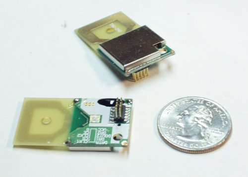
The next step was obviously to incorporate the Nordic IC and circuitry onto the same board. This board was our first attempt at soldering the nRF2401 and surrounding 0603 components. It was poorly laid out (for 2.4GHz freq!) and used a rather large 16MHz crystal, and QFN packaged 16F88. This device was to use a Nordic RF circuitry, and PIC, to wirelessly transmit accelerometer data. We used this board to prove the nRF circuitry as well as develop a new product. Notice the lack of antenna - there was supposed to be a piece of wire-wrap-wire that would be soldered onto the board near C11. Much to our surprise, the board worked! We were able to actually get this thing to talk to our original module-based SMiRF. Excellent! The board emitted enough RF noise that it probably wouldn't pass FCC testing. Range was limited to about a meter, but it worked!

So we quickly rev'd the board to include a power switch (what a crazy idea), status LED (handy), PCB trace antenna, and a smaller and much cheaper 16MHz resonator. The board didn't work. So we trouble shot the board, checked the connections, re-checked, re-programmed, nothing. So we built a second board - tediously checking everything. Nothing. This was a painful lesson on the difference between a resonator and a crystal. The Nordic IC requires 16MHz clock source to operate. The clock needs to be within 20ppm (parts per million) so that two units can understand each other at 2.45GHz. This is a pretty tight tolerance, but obviously needed for such high frequency communication. A resonator is a piece of ceramic cut in such a way that it shakes or 'resonates' at a given frequency. The process is much cheaper than the equivalent quartz crystal process. However, where the quartz crystal can be created with 20ppm tolerance, a resonator can only achieve +/-0.5%. 20ppm is +/-0.00002%. Ahah! The board is functioning just fine, but the 16MHz resonator is so sloppy, no two Nordic circuits can talk to each other. AHHHH.

So a quick retro-fit of the original 16MHz quartz crystal and the board came to life. What a great sanity check that was. So this proto taught us that the nRF circuitry would work, the PCB antenna worked well enough (limited but ok range of 10-15 meters), and we would need to find a suitable 16MHz SMD crystal that was smaller, and slimmer in height.

And here is the eventual super slim design. Date your boards - we forgot to. This design was fabbed around 9-15-04. This is a rather small design constituting an accelerometer, controller, battery, and RF link. Sound familiar? This is basically a foot-pod like the Nike+iPod thing or the ANT based Garmin Forerunner.

Here was the collection of boards that got trashed because of the faulty resonator design.

Here are the protos for the SMiRF with etched antenna. We found that this lump-node antenna didn't help our reception range so we resorted back to the trace antenna. The boards did work however! Sometimes I really miss the days of shiny leaded solder...

The 'final' rev. Here you can see the USB populated board with stub trace antenna using a larger 16F688 PIC (and a small jumper wire fix). Worked well enough, but the firmware was always a problem. You really couldn't push the data rate past 9600bps and the system would drop packets if the range was any more than 20-30 feet. This was a hassle. Around this time we started experimenting with the Bluetooth module from Mitsumi.
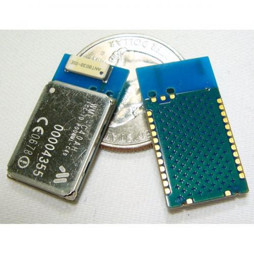
This Bluetooth module was a pre-packaged solution to our serial cable replacement problem. It was everything the SMiRF was trying to be, just with a whole team of Mitsumi engineers behind it. The cost of this module is much higher than the part costs of the Nordic solution, but when the development cost was weighed against the low-purchase volumes, we decided to abandon the fun SMiRF and created the BlueSMiRF based on this technology. Works great!
- Page 1 - The general collection
- Page 2 - The development cycle that started SparkFun Electronics
- Page 3 - The epic progression of the BlueSMiRF
This constitutes a small portion of the hard work we put in here at SparkFun Electronics. Thanks for checking us out! Please use this information at your own risk.
January 7th 2007
Cool
Question. In your article, you state "Date your boards" yet I have not seen any designs, schematic/board or actual product that has a date on the board. Did you eventually abandon dating? I use an SVN server to manage my designs, and always print the REV # on my boards, that way I know which schematic they came from.
You have to look close, but there's a few date codes in there (http://www.sparkfun.com/tutorial/Prototyping/Nordic-RF/P1030060.jpg) For years we have put a date code on the PCB (usually the back side in copper) to keep track of the hardware revision. We're currently getting away from a date code and moving to a 'real' revision #, but it's always fun to flip over a PCB and realize that it was built some previous year. Oh those were the days...
Great tutorial as ever nate.
Thanks!
I rue the day that I discovered this cheaper alternative called the "ceramic resonator". The number of problems that I have eventually traced back to their lack of both precision and accuracy... it's mind bottling.
and mind boggling