Top 10 Design Mistakes to Avoid When Developing your Electronic Hardware Product

Check out the third part in our guest blog series from John Teel of Predictable Designs.
For the next few weeks, John Teel, Founder of Predictable Designs, will be sharing a series of guest blog posts with us, helping readers gain insights into strategy, design thinking, and how to get great product ideas to market. John is an electronics design engineer, serial entrepreneur and blogger, who now focuses on helping hardware entrepreneurs, startups and small companies through his Hardware Academy program. Check out his website for more insights and to learn more.
When developing and selling a new electronic hardware product there are often mistakes made that cost you both money and time to market. I’m going to share with you some of the most common mistakes made when developing a new electronic product, so you can hopefully avoid them during your own product development. This list includes technical errors with your product’s electronics design and mistakes made with the plastic enclosure design in regards to manufacturability. I also include some more general product development mistakes often made by first time developers and entrepreneurs.
#1: Failing to Design for Manufacturing
People tend to underestimate the complexity of developing a new physical product, and they underestimate the complexity of manufacturing it even more. For many products it takes nearly as much time, sometimes even more, to get manufacturing up and running as it does to develop the product. Manufacturing setup can also cost as much or more than all your development costs. It is essential that manufacturability be a primary consideration during the entire product design process. This process is called Design-For-Manufacturing (DFM). Nothing will slow down your path to market more than designing a product that can’t be efficiently manufactured.
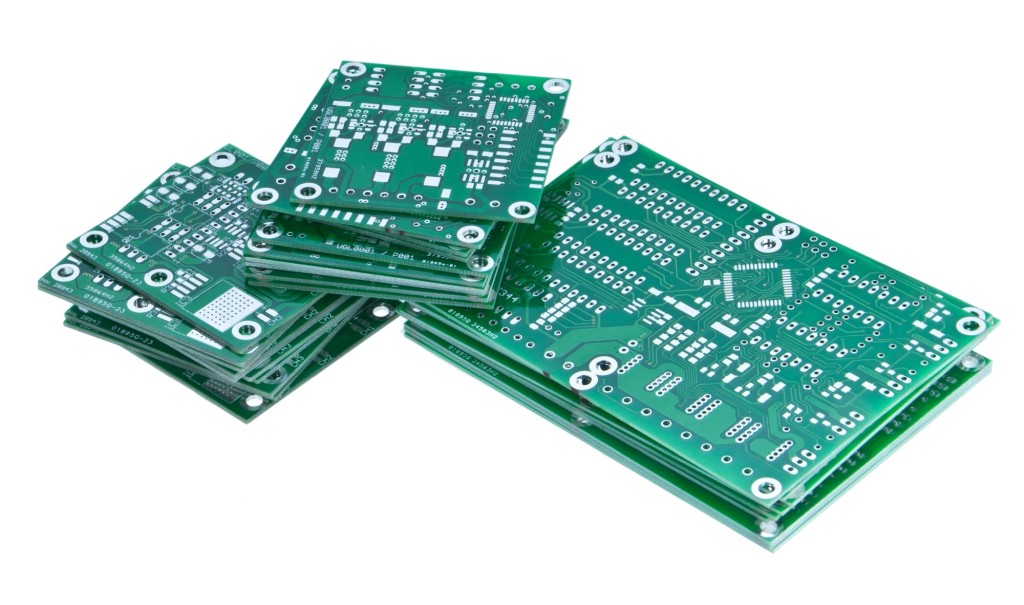
The old way of thinking was that engineers develop a product, and then pass it on to a manufacturer (or the manufacturing department for big companies) who would then figure out how to actually make it. There was little to no interaction between engineering and manufacturing. But that’s a horrible way to develop products, which is why successful companies have abandoned this process. It’s much better to develop a product with manufacturing in mind from the beginning. For example, a simple design change can have a huge impact on making the product easier and faster to manufacture. For most products, two of the primary manufacturability requirements are that the electronics be designed for testability, and the enclosure be designed for injection molding.
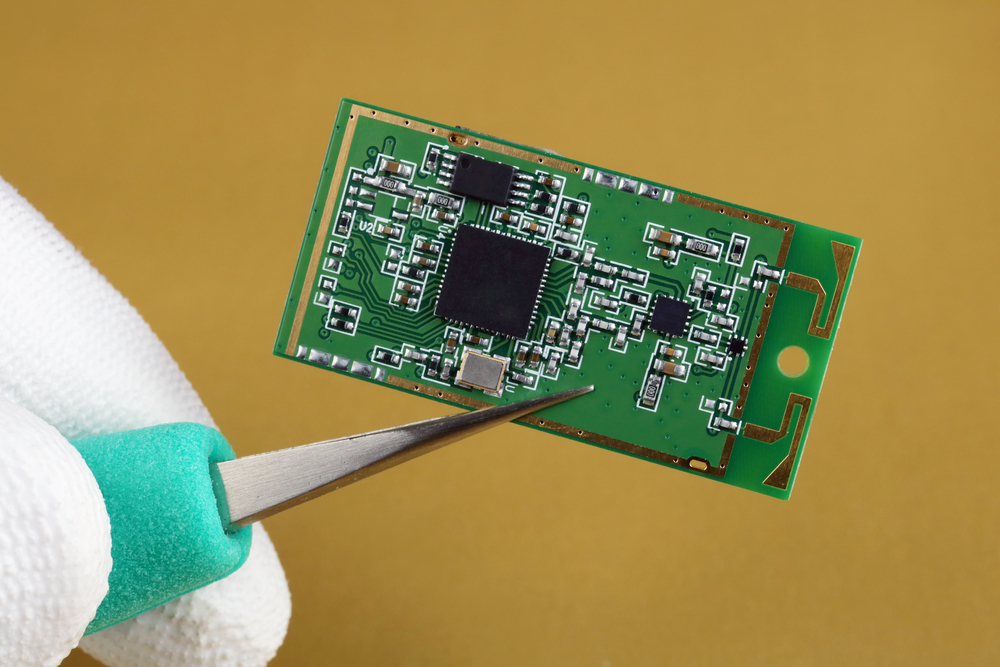
#2: Incorrect Design of Wireless Circuits
If the product has any wireless functionality, the PCB layout for any RF (radio-frequency) portions is super critical. Unfortunately, it’s done wrong more often than right, so watch this one very closely. For example, for maximum power transfer between the transceiver (transmitter/receiver) and the antenna their impedance must be matched. This means two things are required.
First is a proper transmission line connecting the antenna and the transceiver. This transmission line is fabricated on the PCB specifically for carrying microwaves (high frequency radio waves). There are two common types of transmission lines used on PCB designs: a microstrip and a coplanar waveguide. A microstrip is a conducting strip separated by a dielectric layer from a ground plane beneath it. A coplanar waveguide is similar to a microstrip except that it also adds another ground plane beside the conducting strip on the same layer. Of the two styles, the coplanar waveguide is the most frequently used.
In most cases the transmission line needs to be designed with a 50 ohm impedance for maximum power transfer with the antenna. Don’t confuse this impedance specification with the simple resistance of the line. The 50 ohm impedance refers to the complex impedance from the transmission line to the surrounding ground planes. I suggest you use a free tool called AppCad from Broadcom for calculating the proper transmission line dimensions.
In addition to using a 50-ohm transmission line, it’s also necessary to usually add some type of LC matching circuit like a pi-network. This allows fine tuning of the antenna impedance for optimum matching and maximum power transfer.
One of the best ways to avoid these complexities, as well as reduce the cost to get your product certified, is to instead use a pre-certified module for any wireless functions.
For most wireless functions there are two general design strategies: custom build your own circuit using the appropriate microchips, or use a pre-certified module with proven functionality. Designing your own wireless RF circuit is complex. In fact, it is likely the most complex type of circuit to properly design. Honestly, odds are it won’t be done correctly. You should expect to need multiple prototype iterations to get it just right. The other downside to a custom design is it will add at least $10,000 to your FCC certification costs. Use of a module may cut into your profit margin a bit, but maximizing margins should never be your initial priority.
Yes, you need to understand in advance what your profit margins will be once you reach manufacturing at large scale. But when first starting out your priority should be reducing your cost to market, not maximizing your profits. Profit comes later.
#3: Waiting Too Long to Estimate Manufacturing Cost
This is a big one. Successful tech companies always know approximately how much a product will cost to manufacture well before they begin full development. Otherwise, how can they know the product is worth developing?
If you’re not a billion dollar tech company, the odds are you will first get your product fully designed. Once you have the final prototype, and you are ready to start manufacturing, then you will finally estimate how much the product will cost to manufacture. What happens, though, if you discover that your product is going to cost more to manufacture than you expected? You could increase you sales price target, but that obviously has negative consequences.
You could also make some redesigns to lower the manufacturing cost. But wouldn’t it have made more sense to just design it right the first time? For understandable reasons, many people think that you have to fully develop a product before you can accurately calculate the manufacturing cost. That is absolutely untrue. With the right experience, it is possible to accurately estimate the manufacturing cost for just about any product. This can happen well before any PCB layout or 3D modeling occurs.
#4: Insufficient Width for High-Current PCB Traces
If a PCB trace will have more than roughly 500 mA flowing through it, then the minimum width allowed for a trace probably won’t be sufficient. The required width of the PCB trace depends on several things including the thickness of the trace (copper weight), and whether the trace is on an internal or external layer. For the same thickness, an external layer can carry more current for the same width than an internal trace, because external traces have better air flow allowing better heat dissipation.
The thickness depends on how much copper is being used for that conducting layer. Most PCB manufacturers allow you to choose from various copper weights from 0.5 oz/sq. ft to about 2.5 oz/sq. ft. If preferred, you can convert the copper weight to a thickness measurement such as mils. When calculating the current-carrying capability of a PCB trace, you must specify the permissible temperature rise for that trace. Generally, a 10 C rise is a safe choice, but if you need to squeeze down the trace width more you can use a 20 C or higher allowed temperature rise. Although the calculations for trace width are pretty simple I usually recommend using a trace width calculator.
#5: Not Getting a Design Review
If you don’t get an independent design review of your product before you prototype it then you may be throwing money away. It doesn’t matter how good an engineer may be, nobody is perfect, and all engineers make mistakes. Getting custom prototypes made (whether it’s the electronics PCB or the product’s enclosure) isn’t cheap. The more prototype iterations you require, the more it will cost in total. It will also take longer to develop and bring the product to market.
One of the best ways to reduce the number of prototype iterations required is to get a second opinion called a design review. Successful tech companies always require their engineers to hold design reviews to seek feedback from as many other engineers as possible. Unfortunately, many entrepreneurs, startups and small companies make the mistake of completely skipping this critical step. That’s fine if you have the skills to sufficiently review the design yourself. But if you had those skills you would have likely just done the design yourself.
#6: Incorrect Use of Decoupling Capacitors
Critical components need a clean, stable voltage source. Decoupling capacitors are placed on the power supply rail to help in this regard. However, for decoupling capacitors to work their best they must be as close as possible to the pin requiring the stable voltage. The power line coming from the power source needs to be routed so it goes to the decoupling capacitor before going to the pin needing a stable voltage.
Also, it’s critical to place the output capacitor for the power supply regulator as close as possible to the output pin of the regulator. This is necessary for optimizing stability (all regulators use a feedback loop that can oscillate if not properly stabilized). It also improves transient response.
#7: Product Enclosure is Not Manufacturable
You’ve spent all of the time and money getting the design of your product’s enclosure to look just right. It’s like a work of art to you, and this required a bunch of 3D-printed prototype iterations to perfect its look and functionality. You finally have the perfect prototype! Now you just need to find a manufacturer to produce them in mass, and you are good to go. Right? What if I told you that your enclosure design is useless and you need to essentially redo the entire thing? That would be horrible to hear, but this is a very common occurrence.
3D printing is very forgiving. You can design and print just about anything your mind imagines. But 3D printing is only for producing a few prototypes. High-pressure injection molding is the technology used for producing plastic parts in high volume. Unfortunately, injection molding is not at all forgiving. It is a technology with many design rules that must be closely followed. These rules can be so major, and so limiting, as to require a major redesign just to make an enclosure manufacturable. When designing your product’s enclosure be sure to consider injection molding requirements from the very beginning.
#8: Incorrect PCB Landing Patterns
All PCB design software tools include libraries of commonly used electronic components. These libraries include both the schematic symbol, as well as the PCB landing pattern. All is good as long as you stick with using the components in these libraries. Problems begin when you use components not in the included libraries. This means the engineer has to manually draw the schematic symbol and the PCB landing pattern.
It’s very easy to make mistakes when drawing a landing pattern. For example, if you get the pin-pin spacing off by a fraction of a millimeter, it will make it impossible to solder the part on the board. A handy trick to avoid this mistake is to print out your PCB layout at a 1:1 scale. Then order samples of all of the various components (mainly the microchips and connectors), and manually place them on your printed PCB layout. This allows you to very quickly verify that all of the landing patterns are correct.
#9: PCB Design Is Not Manufacturable or Too Expensive
A via is a conducting hole in a PCB that connects signals from different layers. The most common type of via is known as a through via because it goes through all layers of the board. This means even if you only want to connect a trace from layer one to layer two, all of the other layers will also have this through via. This can act to increase the size of a board since the vias reduce the routing space on layers not even using the via. A blind via, on the other hand, connects an external layer to an internal layer, and a buried via connects two internal layers. However, blind and buried vias have very strict limitations on which layers they can be used to connect.
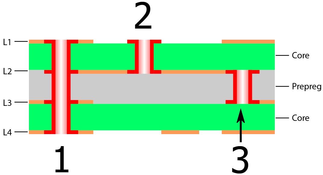
It’s all too easy to use blind/buried vias that can’t actually be manufactured (or prototyped). To understand the limitations of buried and blind vias you must understand how the layers are stacked to make the PCB. Be warned though that even if you use them correctly, blind/buried vias drastically increase the cost of prototype boards. Many times, their use will double your board cost, although this cost increase will be less significant once you reach higher production volumes. In almost all cases, it is best to avoid the use of buried and blind vias, unless you absolutely must have the smallest PCB design possible.
#10: Incorrect PCB Layout of Switching Regulators
A switching regulator converts one supply voltage to another by temporarily storing energy and then releasing it to the output in a controlled fashion. The storage elements used are inductors and capacitors. Compared to simpler linear regulators, switching regulators are extremely efficient and waste very little power. However, they are much more complicated to use correctly. The biggest complexity of using switching regulators is correctly designing their PCB layout. You can’t randomly lay down the components and connect them up. There are strict layout rules you should follow for switching regulators. Fortunately, nearly all datasheets for switching regulators will include a section discussing the proper layout, as well as giving an example of how to do it correctly.
Conclusion
This list could easily be expanded and there are nearly an infinite number of mistakes waiting to be made! Your best bet is to always know about any potential pitfalls well before you actually reach them. This way you can either avoid them completely, or at least be better prepared when they occur.
Hopefully this article helps you eliminate some of these potential mistakes. However, the best way to avoid these types of mistakes is to work with experts. It’s always best if you bring on the necessary experts from the start to help guide you along so you can avoid many of these mistakes before you go to far down a rabbit hole. At the very least, you need to get independent experts to review your design before spending significant money on prototypes or production.
This article was originally published at PredictableDesigns.com.


