EasyEDA: Getting Started with SMT Design!
Learn to create a schematic diagram for your project and design your own PCB using surface-mount components!
Welcome back, all! Today we’re gonna continue on our PCB design journey with surface-mount technology, an approach that is often more cost effective, efficient, and space conserving than using traditional through-hole components. If you haven’t already, be sure to check out the first EasyEDA blog post to get set-up and we’ll dive right in!
Placing Components in our Schematic
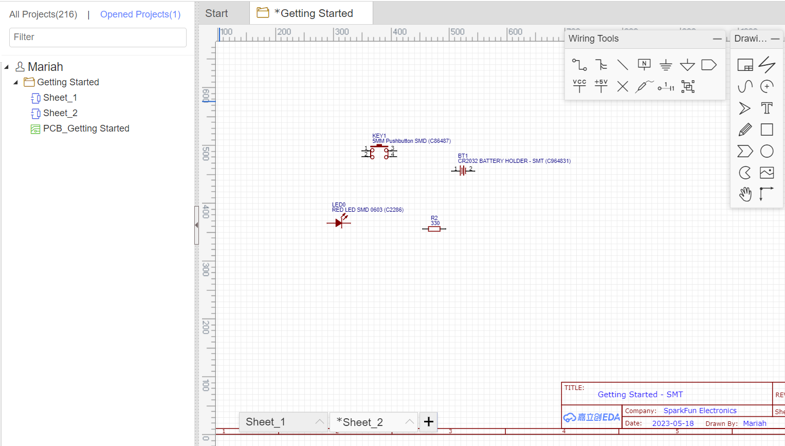
Ok, so, just like last time we’re gonna open up the EasyEDA designer and create a new project (I didn’t separate mine in the beginning but go ahead and create a new folder rather than include it with our last board design) and add our components. I will provide the LCSC product codes that I used just to get us moving and good to go, but definitely check out the LCSC website and get familiar with finding what you need.
- Battery: C964831
- Button: C86487
- Resistor: C101329
- LED: C2286
Connecting our Circuit
Alright, so now we’ve got our friends in here and you may be wondering why they don’t look any different from our through-hole parts from before; basically our schematic diagrams don’t change much since we’re more worried about the type of part in this stage. Once we get to the PCB portion you’ll notice the difference! Let’s go ahead and layout and connect our components:
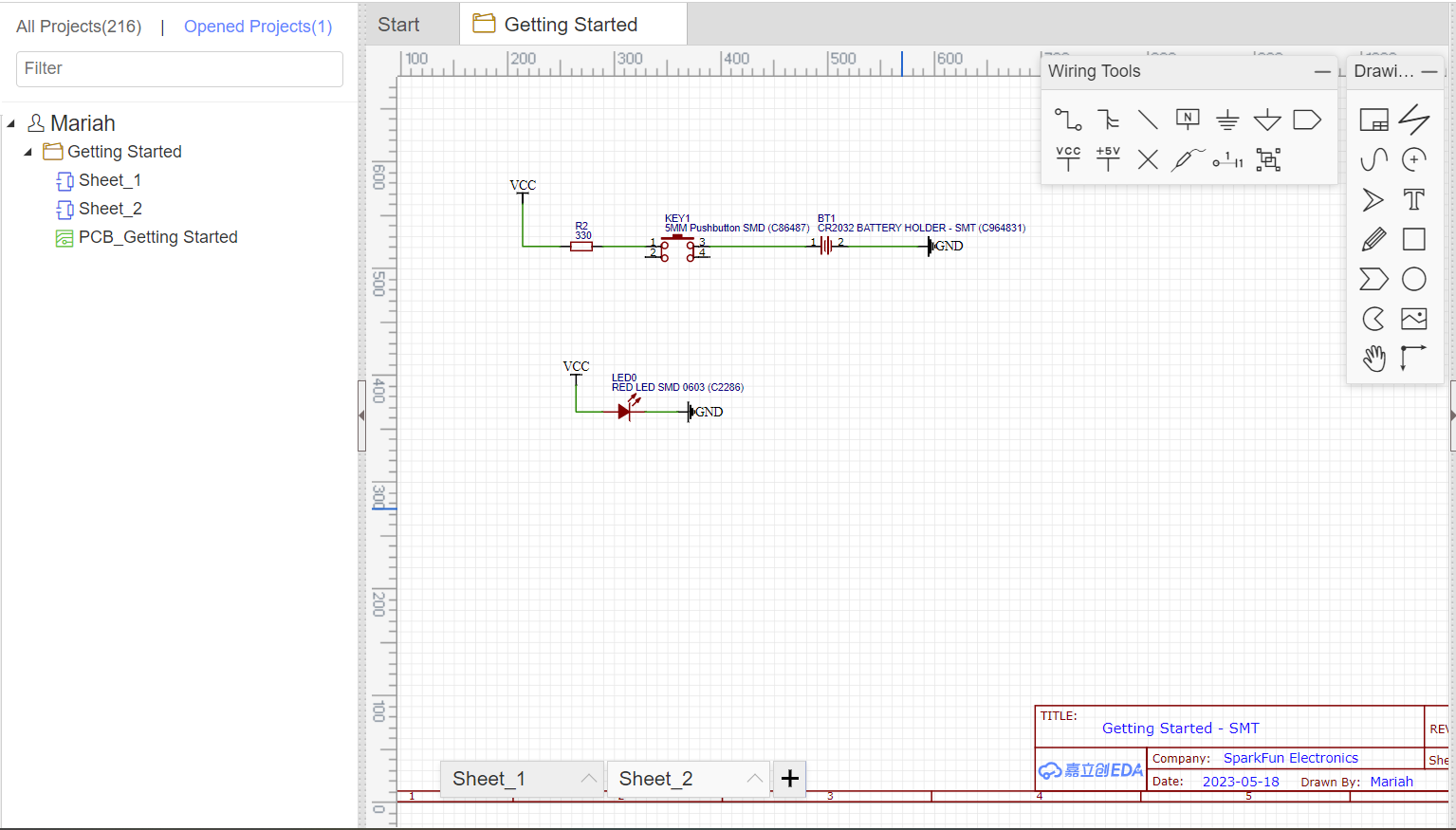
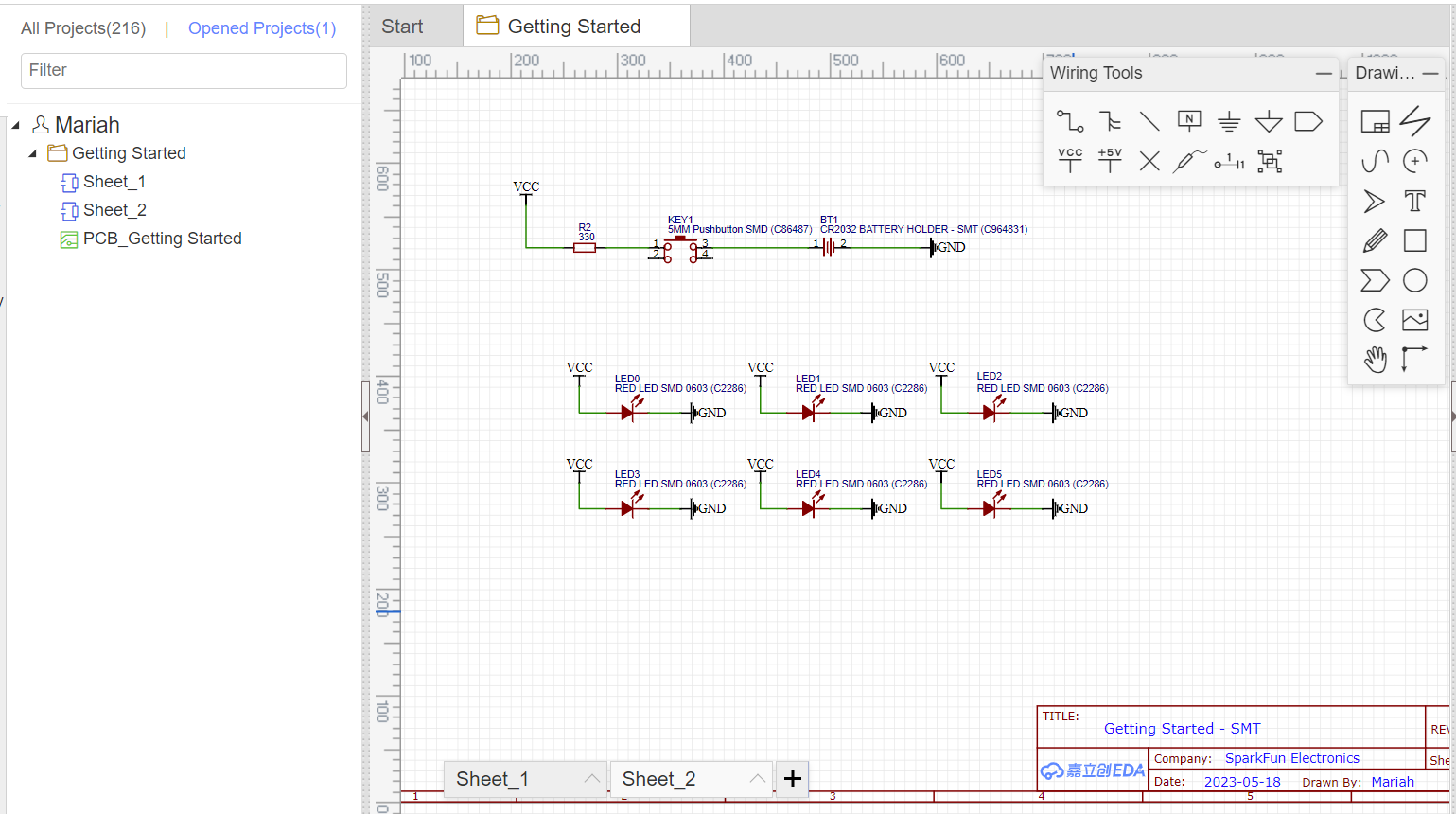
So we’ve connected things a little differently from before and it’ll become clear as to why when we start making traces on our board; for now, I’m gonna throw in some more LEDs for funsies, mostly because the SMT LEDs are very small (we’re using 0603 parts, which is 60 mils by 30 mils, and one mil is 1/1000th of an inch, or 0.001 inches) and I want to take up some more space on our board.
Generating the PCB
Now for the fun part! Let’s go up to the design tab and convert our schematic to a PCB (remember that we’re ok with not checking nets or messing with any of the default settings that pop up here).
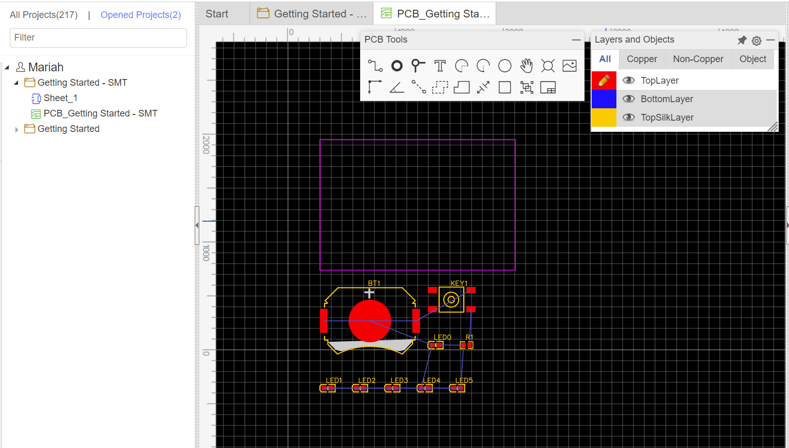
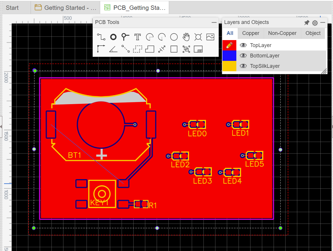
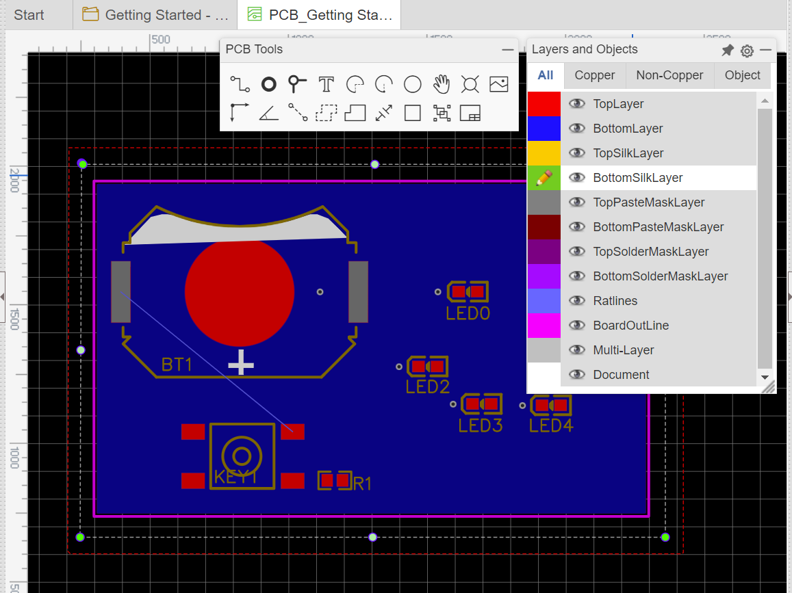
These are surface-mount components! See what I mean about the teeny-tiny LEDs? Let’s lay out our components how we’d like them; one thing to note is that the battery has a curved side and a straight side. The curved side is where the CR2032 battery will slot in, so we want to take that into consideration with how we orient things. I’m going to have it slot in from the top because I want the button to be underneath the battery, so I rotated that part 180 degrees so the button wouldn’t interfere with it. I also arranged my LEDs in a smiley face simply because I can!
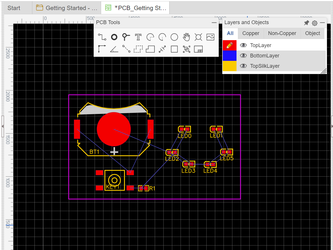
I did have to extend the board outline just a bit to get the look that I wanted, which you can do by selecting the side you want to move and either dragging it with the mouse or using the arrow keys to move it in increments of your snap size. I also went ahead and cleaned up my silk layer as well at this point so that the labels were where I wanted them.
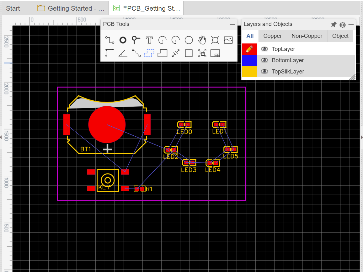
Creating a VCC Plane
Now here’s where things get really fancy; we’re going to create something called a copper area. Essentially what this does is create an entire layer of copper across the entire board; then we can label that area as a connection we intend to make, which allows us to make that connection at any point on the board. It’ll make more sense once it’s there, I promise! So let’s select the tool that looks like a dashed outline of a Tetris piece:
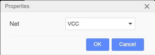
Once you select the tool, a ‘Properties’ pop-up will ask what you’d like the ‘Net’ for this layer to be (a net is a designation that will tell the program what part of our circuit we want it to connect to). We’re going to have this be a VCC plane:
Now, with that tool active, we’re going to click once in all four corners outside of our board outline and right click to exit and build out the layer, like so:
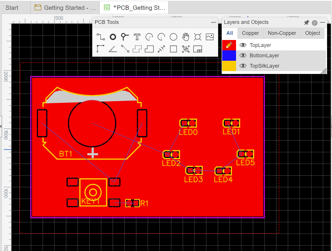
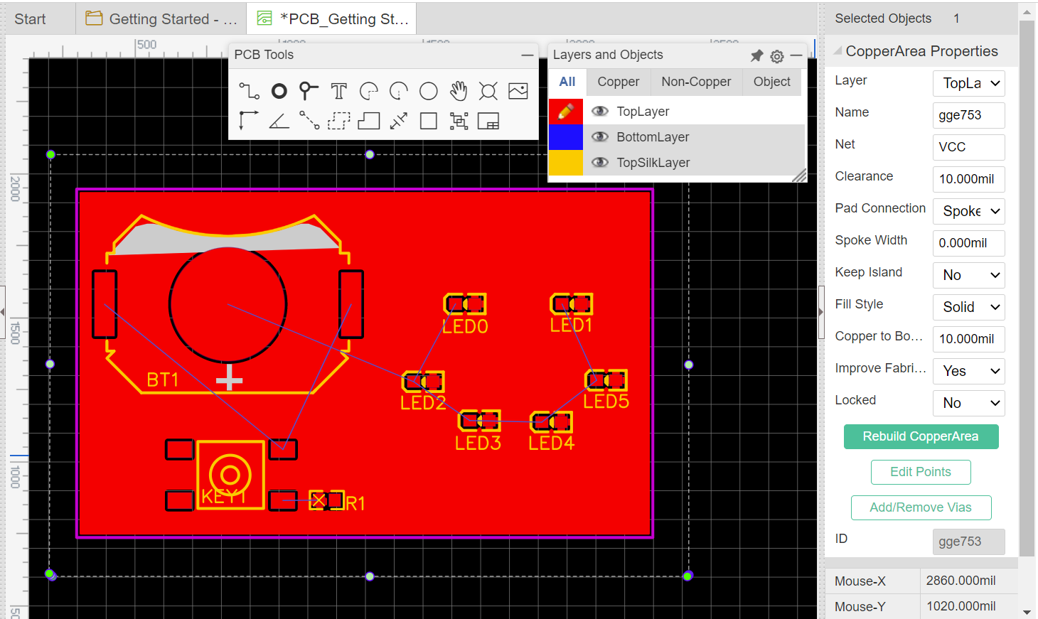
With the copper area filled in, we can see better what it’s doing here: you’ll notice that anything that isn’t connected to a VCC flag on our schematic is isolated from the copper layer and everything that is has a tab-like look on the pad allowing it to make contact with the plane! This really comes in handy with complicated boards and reduces the number of potential crossovers with our traces.
Looking at how I had things laid out and my remaining rat’s nest lines, I realized it’d make much more sense for me to flip my resistor round to make the trace more direct. One thing to note is that the copper layer does not automatically update, so flipping my resistor now means that the pads have changed places and the connections are wrong (you’ll notice the little yellow ‘X’ on one side letting me know that there’s a connection made that I didn’t want). But not to worry! There’s an easy fix to this: click on the dashed outline of our copper area that we drew earlier. On the right side of the screen, you’ll see a button that says “Rebuild Copper Area”; that will regenerate the layer and fix our issue!
Making Traces on the Power Plane
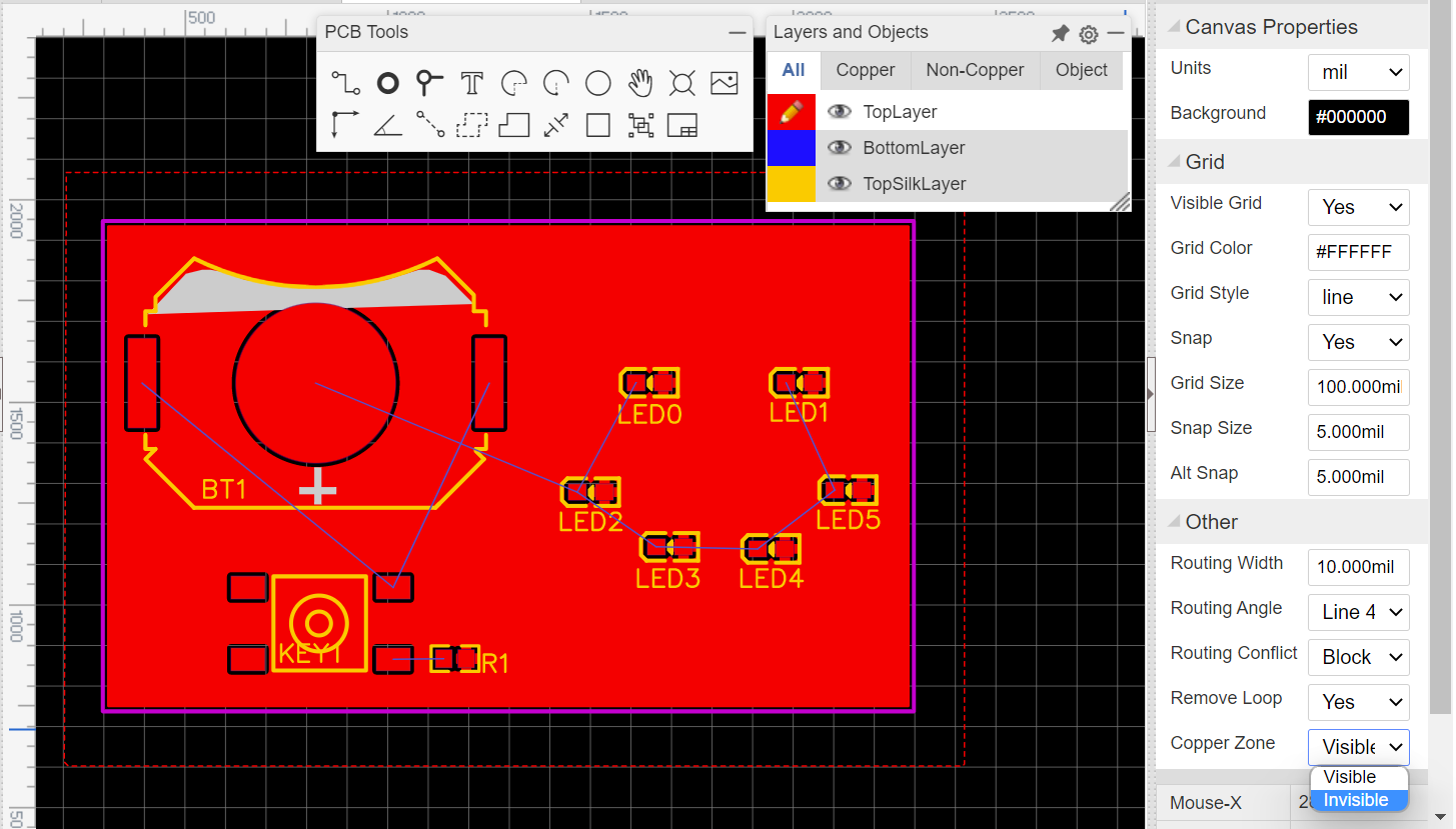
Our VCC is all set, but we still have a few connections left! Let’s look at hooking up our battery, button, and resistor. We could just connect them with the copper layer active, but it can be really hard to see where we’re going in the mess of bright red. On the right side of the screen, you’ll see an option labeled ‘Copper Zone’ (this shows up with the copper area DEselected, so just click off to the side and it should pop up); this menu has a drop down option to make the copper layer invisible, which we’ll go ahead and select so we can see what we’re doing.
With that done now we can create our traces from the battery, to the button, to the resistor. You’ll notice that there are two rat’s nest lines coming from the battery to the button; this is just due to the nature of this part where the two metal tabs on either side are in contact with the positive side of the battery. You can connect both to the button, or one to the other and then to the button, or just one to the button and ignore the other. Totally up to you, I just connected one side and let the other be.
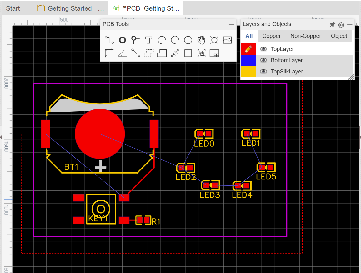
Now that those are good to go, we can rebuild our copper area and turn it back on:

You can even see here how our traces are also isolated from the copper area! I think it has a really neat look.
Creating a GND Plane and Using Vias
Ok! Now all that’s left is to get our GND connections in place and we’re good to go. Let’s make our bottom layer active from our ‘Layers and Objects’ menu, and select the copper area tool again. This time, we’re going to set our net to ‘GND’ and do the same process as before:
Now, until we have a part connecting to the layer, it won’t populate underneath, but I promise it’s there! So, how do we connect something on one layer of the board to the back when it doesn’t poke through the board? Using a super handy tool called a ‘Via’! In the toolbar, it’s the right angle with the small circle in the corner:
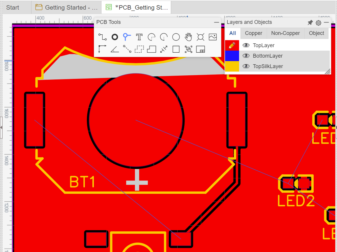
We’re going to place our via next to this big circle in the middle of our battery; what this allows us to do is run a trace from that pad to the via, which will bore through the board and connect it to the GND plane we put underneath!
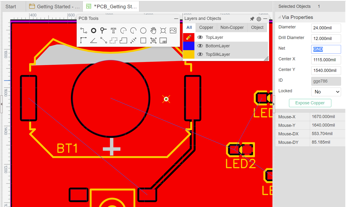
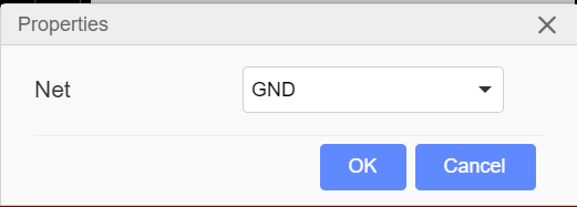
Once it’s placed, select it one more time and change the ‘Net’ on the right hand side to say ‘GND’; this will let the designer know that we want the via to connect to our GND plane on the back, and allow us to run a trace between it and the battery pad.
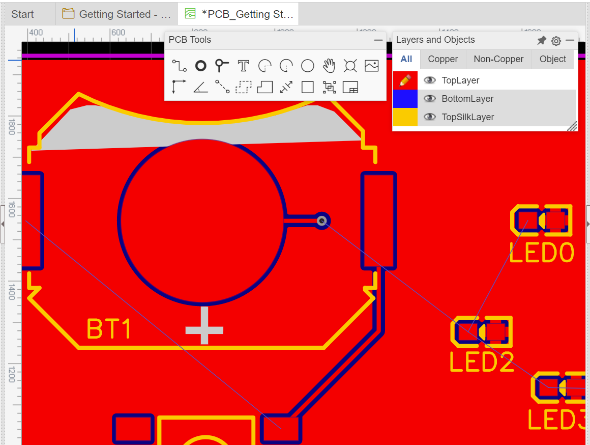
Here’s where we can see the bottom layer plane as that blue area that’s shown up. Told ya it was there! Now all that’s left is to place vias by our LEDs and get them connected to GND as well (thankfully we only have to name our vias once and it will keep the last net entered active). Remember to rebuild BOTH of your copper areas once you’ve made all the connections!
Finishing Touches
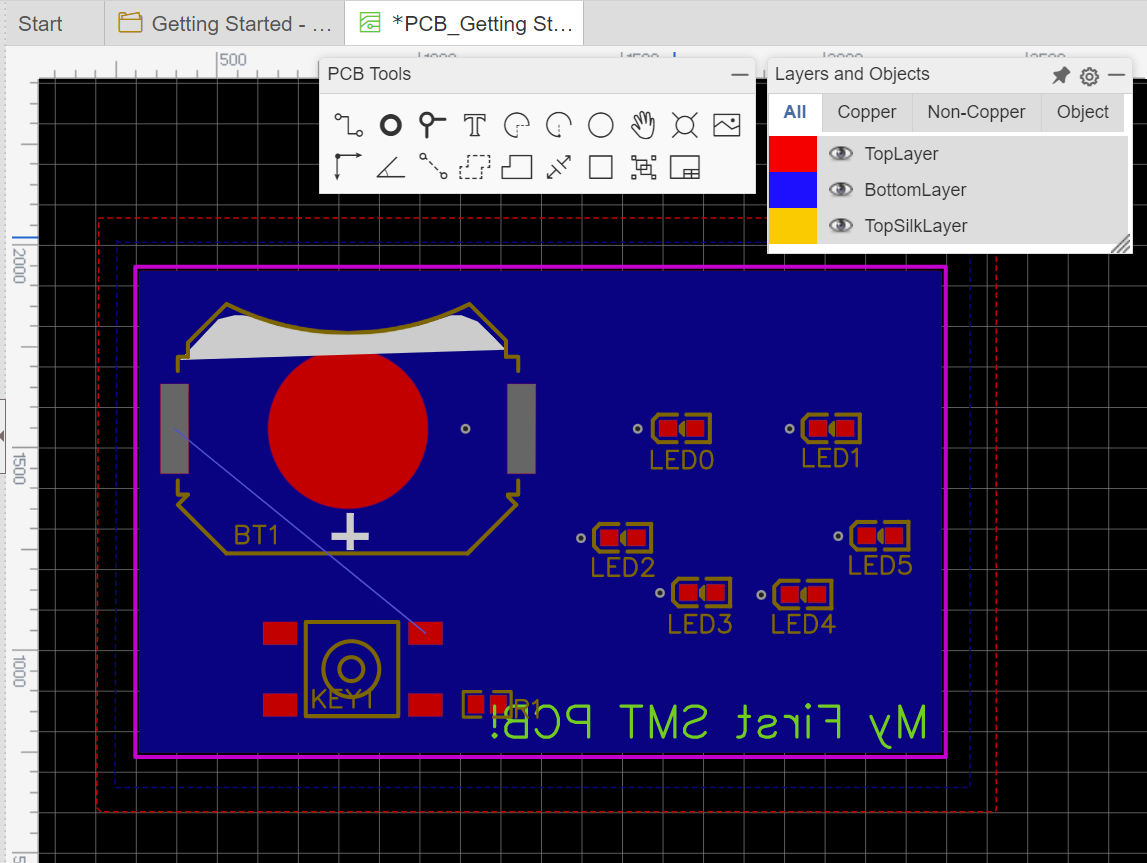
And that’s all there is to it! Let’s slap a label on this bad boy and call it good! This time, we’re going to select ‘BottomSilkLayer’ from the ‘Layers and Objects’ menu.
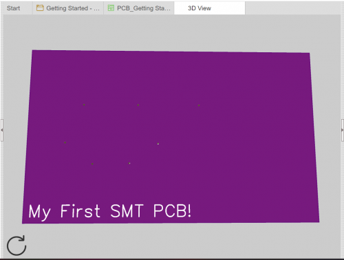
Then, like last time, we’ll select our text tool and write what we want our board to be called (it’ll appear backwards since it’s on the back of our board)!
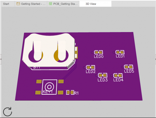
Done! Now let’s check out the 3D view! What’s super cool is that some components have a 3D model so we can see what it will actually look like with the part on the board. I went with purple as the color this time for funsies.
What’s next?
Thank you guys for joining in on getting started with SMT PCB design! As always, let me know if you have any questions or want to see anything in particular and I’ll do my best to make it happen. Come back next time when we’ll explore a bit of the more creative aspects of designing your own PCBs!


