Proto Pedal Example: Analog Equalizer Project
 Byron J.
Assembly
Step Zero
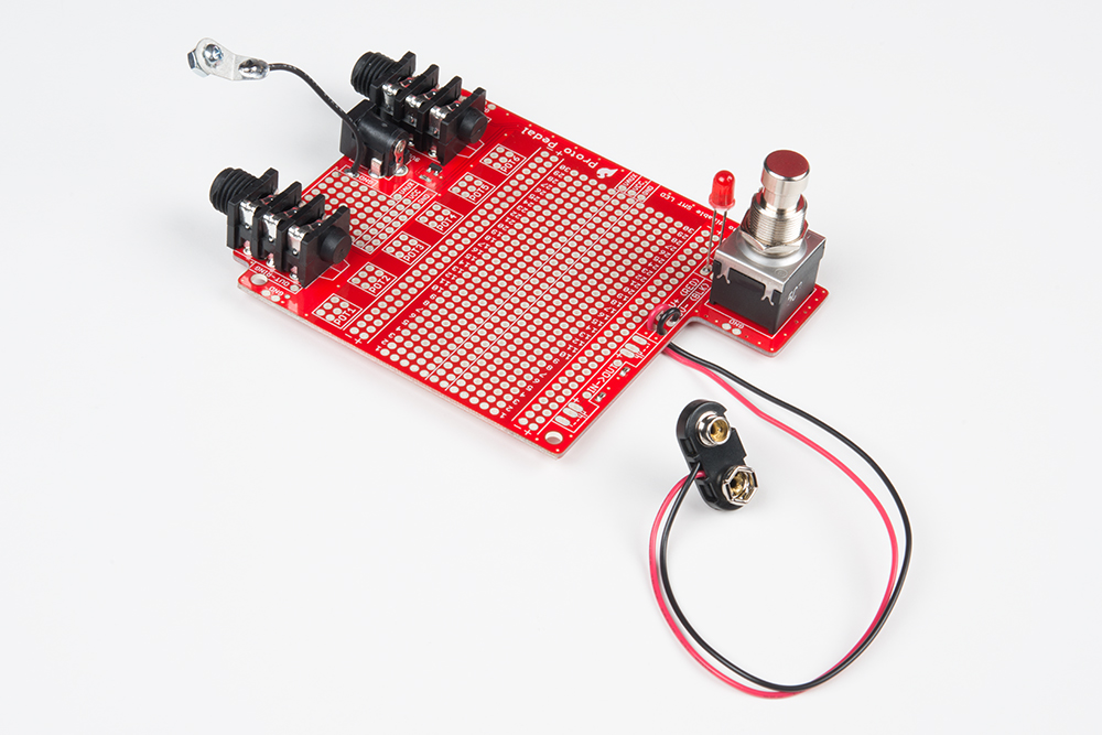
To begin, we'll assume that you've completed the basic assembly of the proto pedal board.
If you're using the Proto Pedal Chassis, you'll need to prepare it by drilling holes for two potentiometers, as shown in the Chassis Hookup Guide.
With the prerequisites complete, you can start the sequence below. We're going to be stepping in fairly large chunks. Each step lists the required components, so you can prepare them before you commence. Once they have been placed, double-check your solder joints, and compare your work to the photos.
Playing Battleship
In the following steps, we're going to use the grid notation seen on a standard solderless breadboard. From left to right, the columns are numbered 1 to 30, and, from bottom to top, the rows are assigned letters from A through J. Any hole in the center of the board can be referenced by number-letter coordinate, such as 27L or 7G.
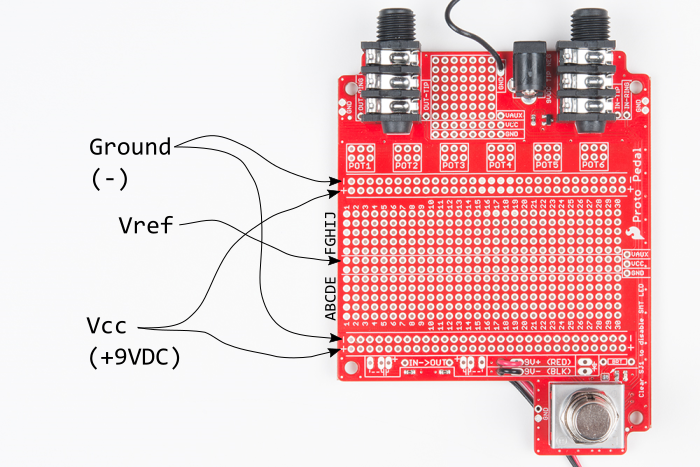
Additionally, we'll be using the power and center rails of the proto area. At the top and bottom edge of the board are 9V power (AKA Vcc) on the traces marked + and ground on the traces marked -. One of the center traces is used as a half-rail bias voltage, which we'll refer to as Vref.
In the following steps, we'll give the coordinate designation of each component.
Step One: Wire Jumpers
The first step is to use solid core hookup wire, and make some basic connections between sets of pads in the proto area. For clarity, we're using many different colors of wire, but not using any red wire.
| Jumper Number | Color | Start Coordinate | End Coordinate |
|---|---|---|---|
| 1 | Black | In | 1A |
| 2 | Yellow | 2A | Lower Vcc |
| 3 | Blue | 3E | 3F |
| 4 | Green | 10J | Upper Ground |
| 5 | Yellow | 11J | Pot3 Left |
| 6 | Black | 12J | Pot3 Right |
| 7 | Blue | 17J | Pot3 Middle |
| 8 | White | 18E | Pot4 Middle |
| 9 | Green | 20J | Upper Ground |
| 10 | Bare | 11D | 12D |
| 11 | Yellow | 12C | Vref |
| 12 | Yellow | 13A | Lower Vcc |
| 13 | Black | 16F | Out |
| 14 | Bare | 22G | 23G |
| 15 | Bare | 21D | 22D |
| 16 | Yellow | 23A | Lower Vcc |
Installed, these jumpers look like this.
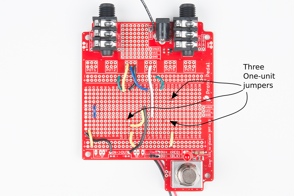
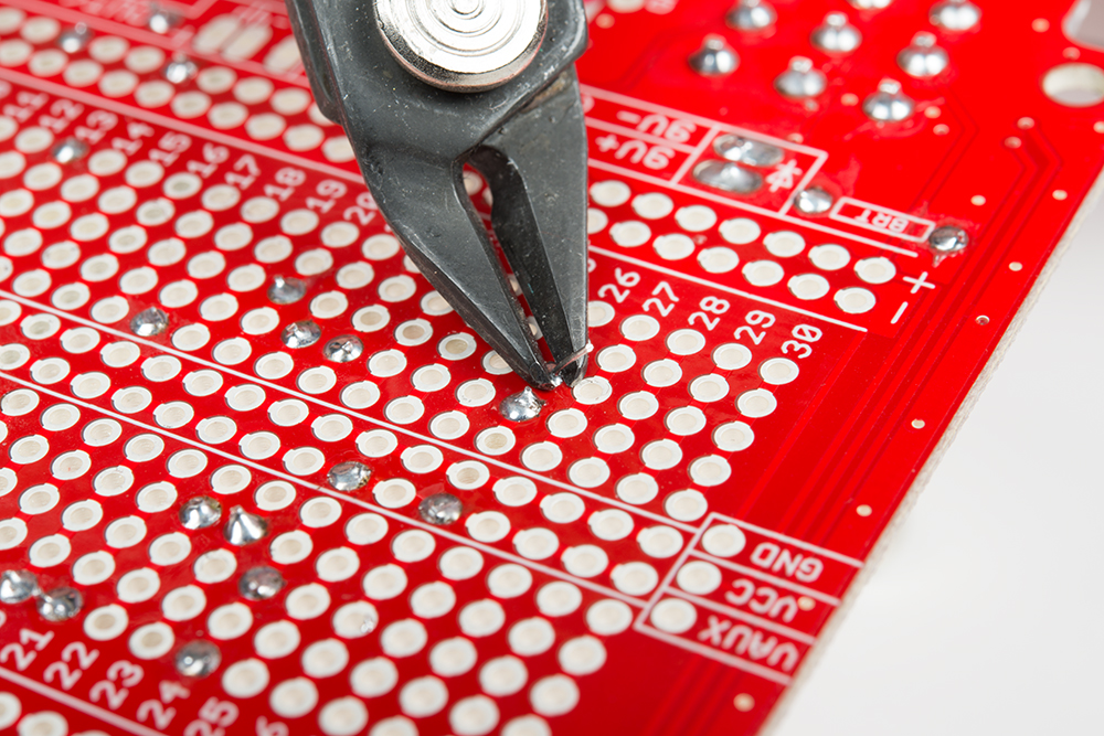
The jumpers are soldered to the back of the board and trimmed close to the board. If the tails stick out too far, they will short to the metal enclosure.
When you're done, count the number of jumpers -- there should be sixteen in total. If you find that you're short, doublecheck that you've got the 0.1 inch wire links as noted in the photo.
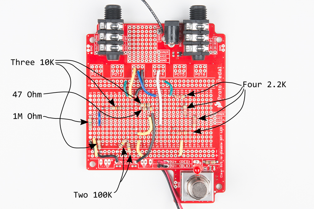
Step Two: Resistors
There are eleven resistors in this design. To get started, select the following from your resistor assortment. We include the color markings below. The packaging of the resistor assortment serves as an illustrated guide.
| Resistor Value | Value Color Code | Start Coordinate | End Coordinate | Placement Notes |
|---|---|---|---|---|
| 1M Ω | brown-black-green-gold | 1D | Vref | |
| 10K Ω | brown-black-orange-gold | 3B | Lower Ground | |
| 10K Ω | brown-black-orange-gold | 4G | 11G | 0.7" long |
| 10K Ω | brown-black-orange-gold | 12H | 16H | 0.4" long |
| 100K Ω | brown-black-yellow-gold | 10A | Lower Vcc | |
| 100K Ω | brown-black-yellow-gold | 10B | Lower Ground | At angle |
| 47 Ω | yellow-violet-black-gold | 13G | 16G | |
| 2.2K Ω | red-red-red-gold | 21J | 24J | |
| 2.2K Ω | red-red-red-gold | 24H | Vref | |
| 2.2K Ω | red-red-red-gold | 26D | Vref | |
| 2.2K Ω | red-red-red-gold | 20C | 26C | 0.6" long |
These resistors get installed as shown below. Take note of a couple placement details: some of the resistors are stretched longer than you might expect, and one of the 100K Ω resistors is at an angle.
Step Three: Capacitors
There are ten capacitors, as follows. The values are printed on the caps, and there is a value decoder on the package. The ceramic caps are the small yellow ones, and the electrolytic caps are small black cylinders.
| Capacitor Value | Value Marking | Start Coordinate | End Coordinate | Orientation Notes |
|---|---|---|---|---|
| 100 pf ceramic | 101 | 12I | 16I | |
| 0.01 uf ceramic | 103 | 18A | 20A | |
| 0.1 uf ceramic | 104 | Input Coupling | ||
| 0.1 uf ceramic | 104 | 22B | 24B | |
| 0.1 uf ceramic | 104 | 24A | 26A | |
| 1 uf electrolytic | 1uf/50V | 17G | 19G | `-` to right |
| 1 uf electrolytic | 1uf/50V | 22I | 24I | `-` to left |
| 1 uf electrolytic | 1uf/50V | 19I | 21I | `-` to left |
| 10 uf electrolytic | 10uf/25V | Output Coupling | `-` to right | |
| 10 uf electrolytic | 10uf/25V | 3H | 4H | `-` to right |
These capacitors are installed as shown below. We've noted the polarity orientation of the electrolytic caps above, also -- the body of the cap has a white stripe with "-" symbols printed to mark the negative leg.

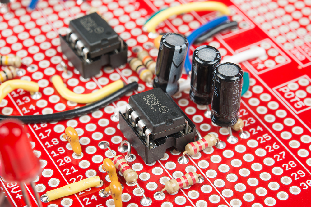
Step Four: Semiconductors
There are two types of semiconductor devices used in this project. The MOSFET is part of the Discrete Semiconductor Kit.
| Component | Marking | Start Coordinate | End Coordinate | Orientation Notes |
|---|---|---|---|---|
| 5LN01SP MOSFET | YB | 3C | 1C | Pin1 in column 3 YB facing upwards rounded edges facing downwards |
| DIP-8 IC Socket for LM358 | Row 10 | Row 13 | Spanning center trough Notch facing right | |
| DIP-8 IC Socket for LM358 | Row 20 | Row 23 | Spanning center trough Notch facing right |

Step Five: Flying Wires & Pots
This last step involves adding the pots to the board. We'll make a little subassembly out of them, then solder that to the PCB.
Because it needs to flex a bit, we're using stranded wire for this step. Cut the following pieces
| Length (Inches) | Lentgh (Metric) | Color |
|---|---|---|
| 2.5" | 5cm | Blue |
| 2.5" | 5cm | Red |
| 2.5" | 5cm | Blue |
| 5" | 13cm | Red |
| 5" | 13cm | Yellow |
| 5" | 13cm | Green |
First, orient the pots so the legs are facing the same direction. If you're using the enclosure, you can put the pots in the chassis holes to hold them in place while you work.
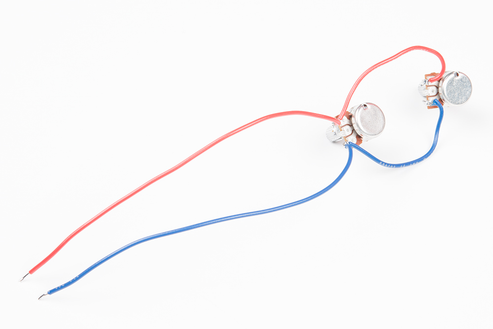
Use the shorter pieces of red wire to jump from pin 1 of the first pot to pin 1 of the second pot. Before soldering tie the longer piece of red wire to pin 1 of the first pot. Then, repeat the above, bridging from pin 3 to pin 3 with blue wire.
Next, solder the yellow wire to pin 2 of the first pot, and green wire to pin 2 of the other pot. The pot with the yellow wire is the low frequency control, and the pot with the green wire is the high frequency control.
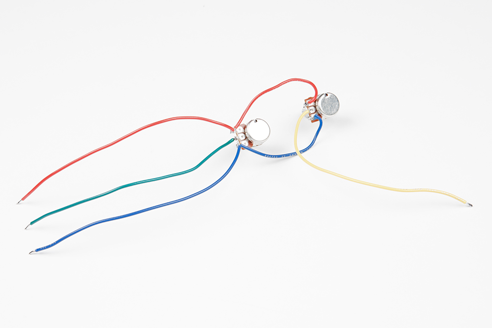
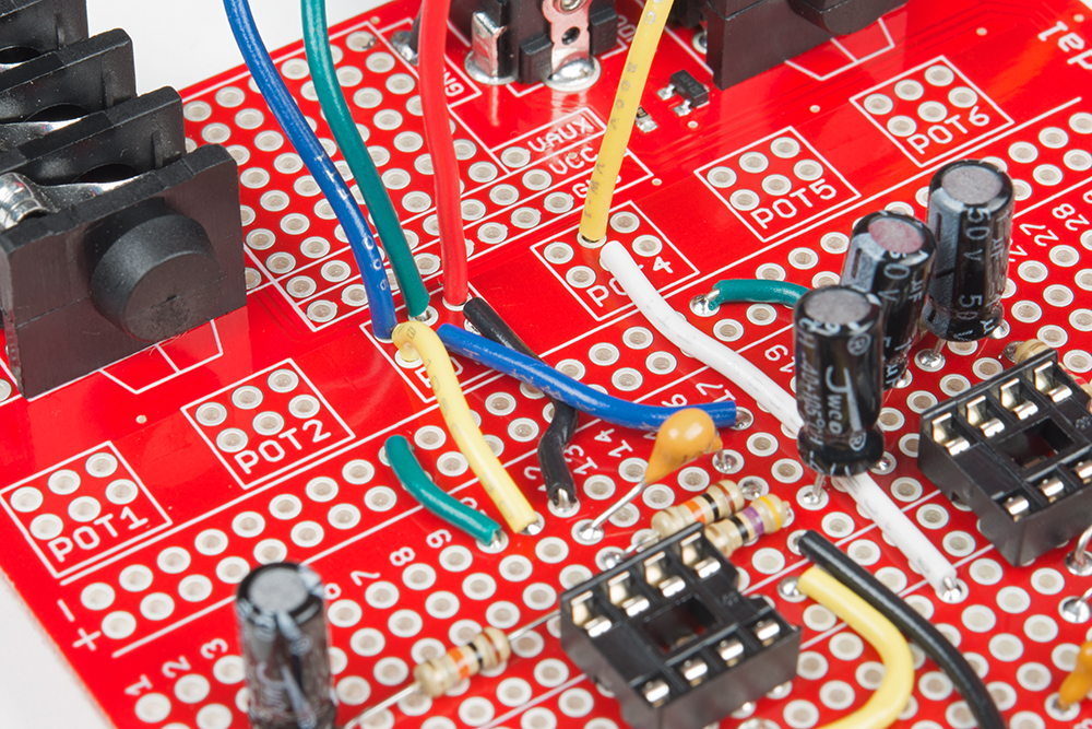
At this point, you'll have four wires trailing from the subassembly. They meet the PCB as shown below, in the pot 3 and 4 areas.
Last Step: Insert the ICs
With the above steps completed, you can insert the IC's in the sockets, taking care to align the pin-1 marks. The dimple should be at the top-right corner, and the notch should be facing right. The legs come splayed out a little bit wider than the sockets -- they'll need to be bent in a little bit to fit.
Now we can move on to testing the pedal!