Enginursday: Using a Motor Driver as a Class D Amplifier

The serial controlled motor driver is stripped of its firmware and reprogrammed to function as an amplifier. Then it's surrounded with circuits that turn the whole shebang into a portable guitar amp.. but it won't win any awards.
This week for Enginursday I use magic and wishes to transmogrify a Serial-Controlled Motor Driver into a Class D audio amplifier. Seriously, though, it's just engineering. After all, a speaker's just a motor that doesn't spin very well.
Theory
The driver can supply 1.2A on each output, and I can bridge those two outputs for 2.4 amps. If I run a 10V supply, I can sustain 24 watts of power to a speaker. With a 4 ohm speaker, the max current draw is 10V/4Ω, or 2.5A. Well, the motor driver can peak 3A, and audio is a series of peaks, so we'll go for 25W of output power. This thing should be loud enough.
Code
Before building anything at all, I wrote the program to prove that this was even possible. (I actually did this awhile ago for another engineer's future post, so stay tuned.) It's important for me to have a plan before doing the fun construction stuff, or I can really get myself into a pickle. So we have to start by talking about code.
Class D audio amplifiers work by supplying a varying PWM output to a speaker. The speaker is an inductive load, so the current can't build up instantaneously, resulting in a filter that resolves the rail-to-rail output voltage back into an analog electromagnetic push on the air. I like to think of it as the current has momentum, and the PWM shoves it up and down as the cycles go by.
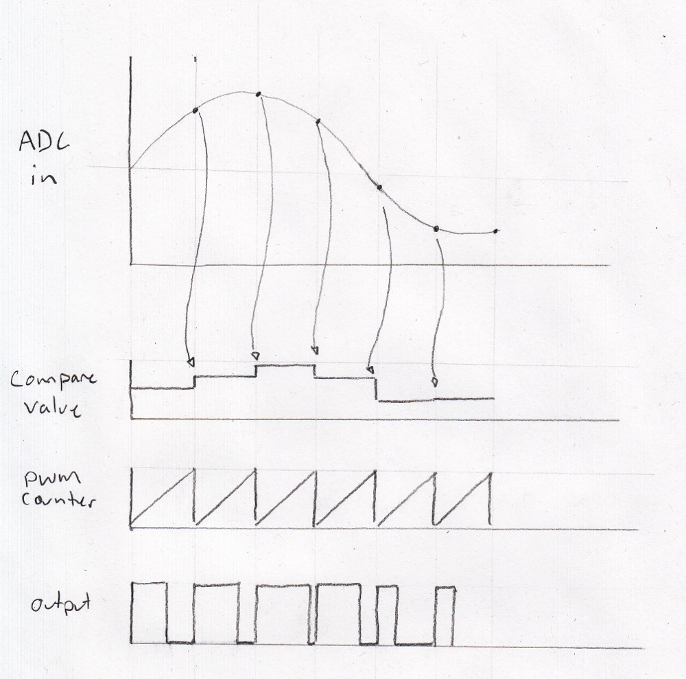
The strategy here is to periodically sample an input pin, then set the PWM compare value (duty cycle) at a fixed rate. An easy task to talk about, but there are some nuances that arise. If the PWM compare value is changed mid-cycle, the output can take on unknown values and have some cycle aliasing going on. The same thing that happens while refreshing LCDs mid-scan.
The solution is to operate synchronously. As soon as the PWM cycle starts, an interrupt is fired. The program transfers the next calculated compare value into the register, and then it samples the ADC and prepares a compare value for the next interrupt. So it's really a synchronous operation with single sample buffer.
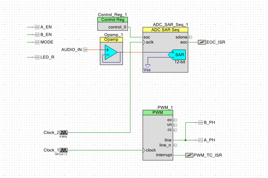
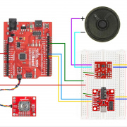
The main thing that sets PSoCs apart from regular microcontrollers is the ability to create peripherals in the logic fabric, so each project includes the logic schematic, along with the code.
The full program listing is only a hundred lines.
#include <project.h>

static void systemInit( void );

uint16_t LED_Counter = 0;
int8_t sampleValid = 0;
uint16_t lastSample = 250;
//Functions
int main()
{
    systemInit();

    while(1)
    {

    }//End of while loop
}

/*******************************************************************************
* Define Interrupt service routine and allocate a vector to the Interrupt
********************************************************************************/
CY_ISR(Sampler_Interrupt)
{
    PWM_1_WriteCompare( lastSample );
    //At top of count,
    //Save old input value
    int32_t nextSample;
    if(sampleValid>0){
        nextSample = (ADC_SAR_Seq_1_GetResult16(0));
        //load PWM register
        nextSample -= (1024 - 7); //now centered about 0
        nextSample = nextSample; //scale
        nextSample += 250; //align to new center
        if(nextSample > 450)
        {
            nextSample = 450;
            LED_R_Write(LED_R_Read()^0x01);
        }
        if(nextSample < 50)
        {
            nextSample = 50;
            LED_R_Write(LED_R_Read()^0x01);
        }
        lastSample = (uint16_t)nextSample;
        sampleValid = 0;
    }

    //Start new conversion
    Control_Reg_1_Write(1);
    Control_Reg_1_Write(0);


    PWM_1_ClearInterrupt(PWM_1_INTR_MASK_TC); //This is early, avoid LED noise

    //Work on LED
    LED_Counter++;
    if(LED_Counter > 48000)
    {
        LED_Counter = 0;
        LED_R_Write(LED_R_Read()^0x01);
    }
}

CY_ISR(conversion_Interrupt)
{
    sampleValid = 1;
}

//get the system off the ground - run once at start
static void systemInit( void )
{

    //Do a boot-up delay
    CyDelay(100u);

    LED_R_Write(1);
    MODE_Write(1);
    A_EN_Write(1);
    B_EN_Write(1);

    //Clock_2
    Clock_2_Stop();
    Clock_2_Start();

    ADC_SAR_Seq_1_Start();
    ADC_SAR_Seq_1_StartConvert();

    /* Start the components */
    PWM_1_Start();
    PWM_1_WriteCompare(128u);
    Opamp_1_Start();

    //Clock_1 is the motor PWM clock
    Clock_1_Stop();
    Clock_1_Start();

    EOC_ISR_StartEx(conversion_Interrupt);
    PWM_TC_ISR_StartEx(Sampler_Interrupt);
    CyGlobalIntEnable;
}
During startup, the clocks are started, pin parameters set, and a couple of ISRs are defined --- one for conversion complete and one for the sample rate.
Conversion Interrupt --- All this does is set a global flag to indicate that the conversion was completed. This flag is cleared when the conversion value is used.
Sample Interrupt --- All the work is done here, at the beginning of each PWM cycle. In pseudo-code, the ISR will:
- Write the last sample to the compare register
- If the last conversion sample is valid:
- Get a new ADC value
- Scale value PWM count size
- Limit range for safety
- Save calculation for the next round
- Start a new ADC conversion
The full PSoC project is available for download. It is made in PSoC Creator 3.3 and targets the PSoC 4245 IC.
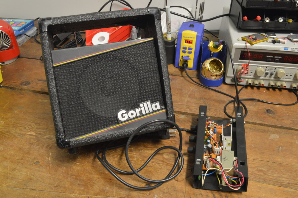
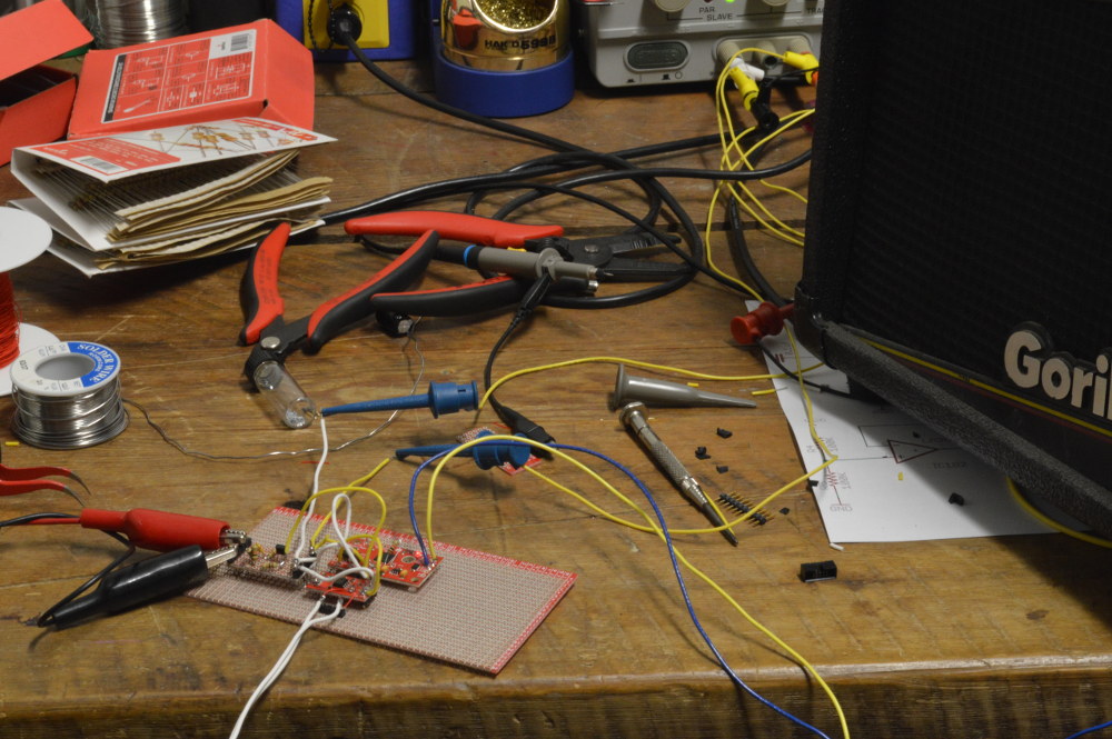
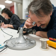
The Build
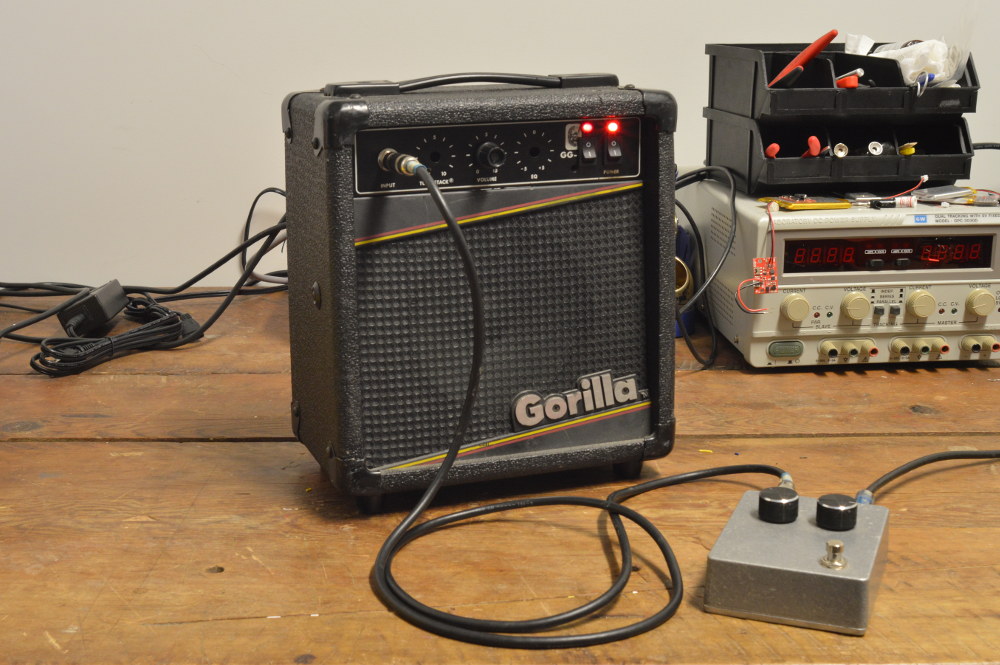
With the core problem solved, I started building circuits and packing them into a chassis. The selected chassis came from a junk heap, broken, and disassembled. The previous owner found that it stopped working and threw it out. The problem was a faulty monolithic amp IC that wasn't worth replacing.

Input Signal Conditioning
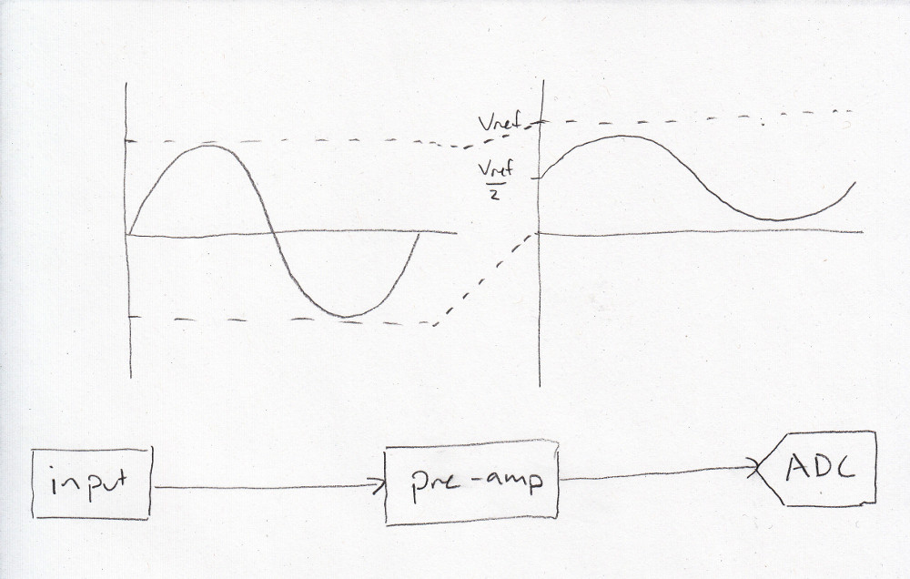
The PSoC's ADC has a range of 0 to 3.3V, but an instrument's output can be over a couple volts, centered about 0V, and with high impedance.
The input circuit will have to present a high impedance to the instrument, have volume control and shift the signal to the ADC range.
Voltage Follower
For the voltage follower, I started from the Analog Equalizer Pedal project's schematic. I printed it out and started making mental modifications, and drew notes.
The schematic is drawn for a guitar pedal running from 9V, and originally had a spare op-amp to buffer the reference voltage. I used two 10k resistors instead, which keeps the input floating around half with the input disconnected. I decided to remove the post-follower coupling capacitor because one is provided by the next stage.
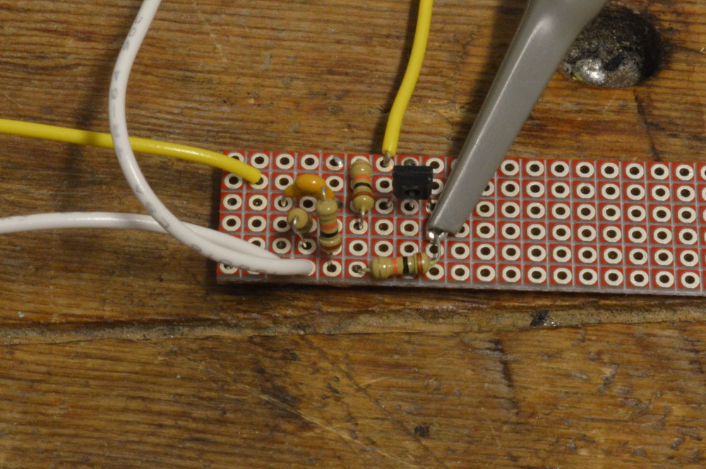
The circuit is constructed on Snappable Protoboard using basic components from the resistor, capacitor and discrete kits.
At this stage, the high input impedance has been converted to a somewhat lower impedance of ~10kΩ, and has a resultant offset. Still the range is not acceptable. There's no gain control, and the center is set to half of the main power rail and not the ADC reference. This is to allow a large input signal to be used, which would be outside the 3.3V constriction of the ADC reference.
Scaling and Offset
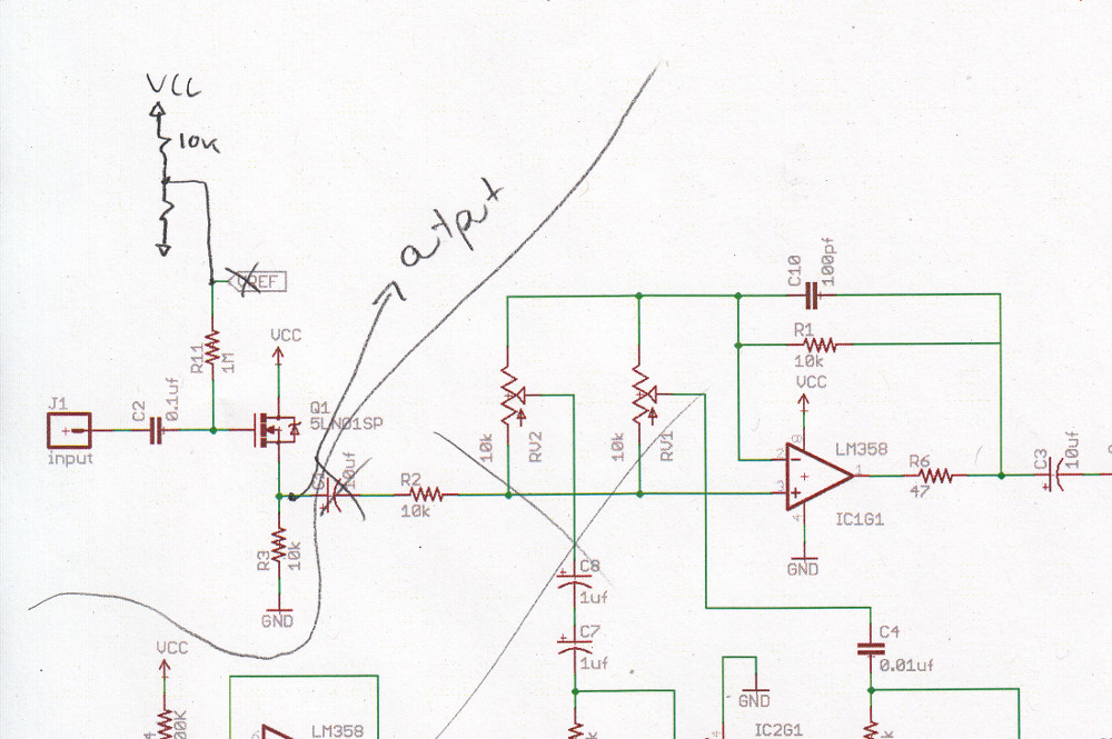
To solve the problems of the previous stage, an op-amp stage is applied. The Op-Amp Breakout has much of the necessary passives and also works rail-to-rail at 3.3V, so it is perfect.
Well, not entirely.
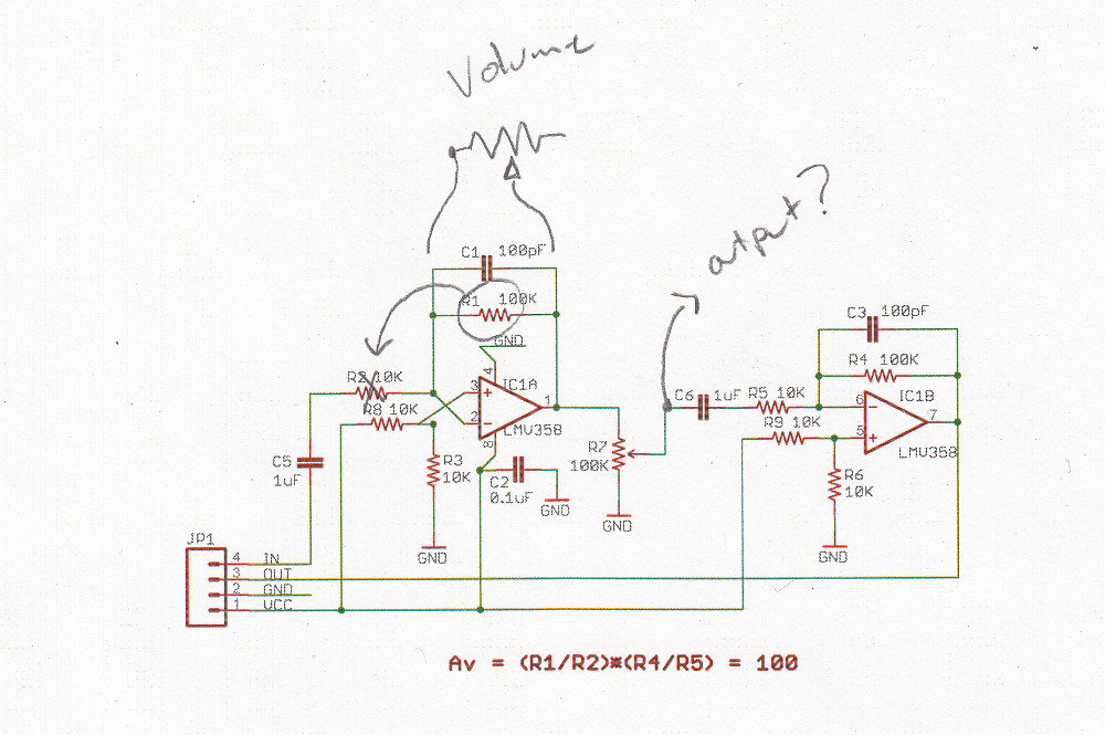
Again, I printed a copy of the schematic so I could keep track of what I was modifying. Whereas most amplifiers amplify, this application calls for attenuation, so I had to move some components around.
The amp came with a 50k potentiometer, so with the 100k feedback resistor moved to the input, the circuit can now operate at a gain from 0 to 0.5. The output could have been pulled from the first op-amp stage, but I found it didn't contribute to the noise, so I left it in. It's also nice to tune the gain after assembly.
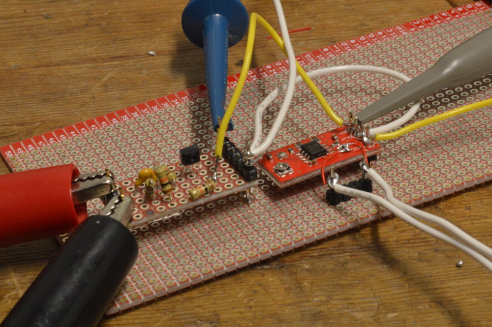
The construction method here is to wire little circuit boards loosely to a larger snappable PCB, then connect with wires. Generally, unused pins go down and mechanically attach the stages, and used pins float upward acting as a terminal strip one might find in an amplifier. This allows rework of the connections.
With the second stage added and tested, the audio can now be passed to the motor driver's ADC input directly.
Amplifier Stage
In order to get the code onto the PSoC, a header is added to the programming port. I use a Cypress kitprog programmer that was salvaged from a BLE dev-kit, though the proper tool for working with the PSoC is the MiniProg3, available from Cypress.
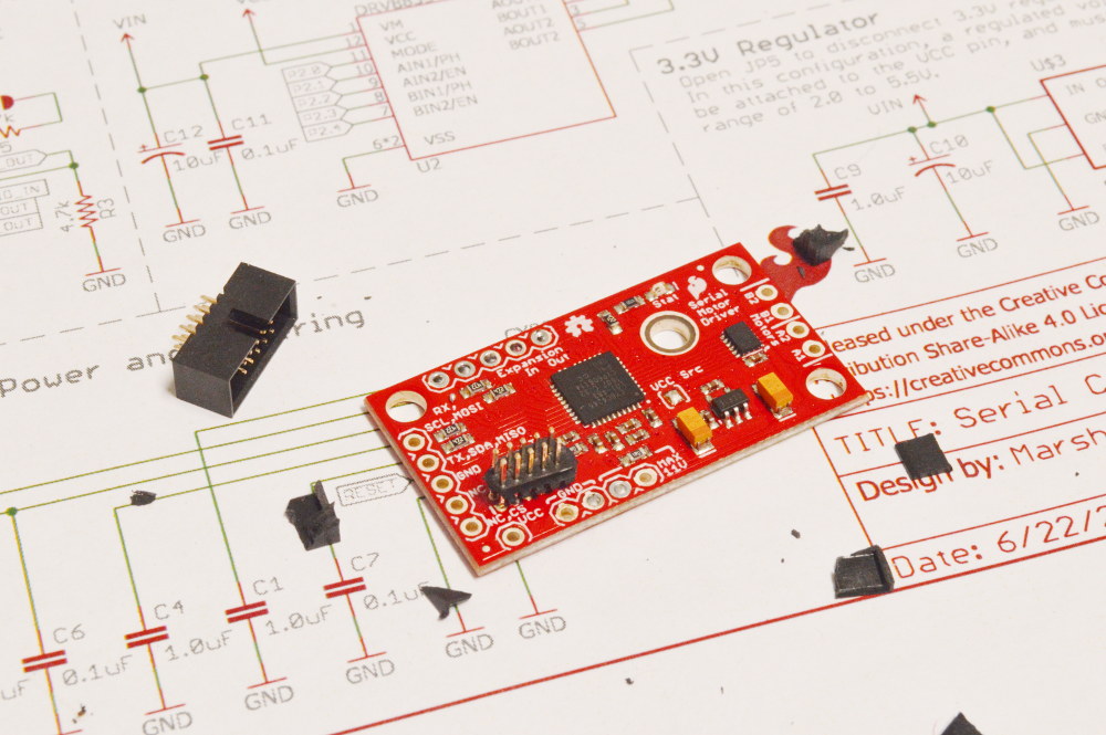
A now unused serial pin is converted to analog input, so there's really no modification necessary other than the addition of the header.
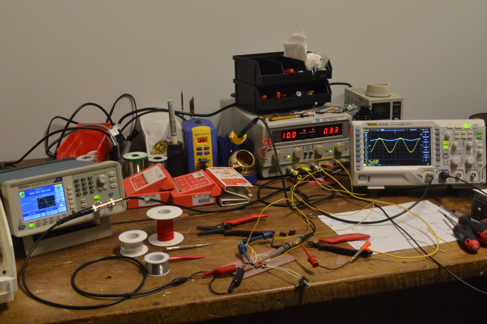
The output of the pre-amp stage is wired directly to the input of the PSoC ADC, a speaker is attached, and the PSoC logic rail is used to power the previous stage at 3.3, ensuring that the range will be appropriate. The circuit now drives the speaker, and it's pretty loud.
With the circuit out on the bench, I thought about how it will be powered. At 5V it's pretty loud, but it's much louder at 10V. So I decided to add the extra complexity of dual battery packs and boosters.
Supplying Power
Two 5V/1A Charger/Boosters are used in conjunction with 6Ahr Lithium Ion batteries. The boosters will be connected in series, meaning each will have a different ground reference; therefore, two switches must be used.
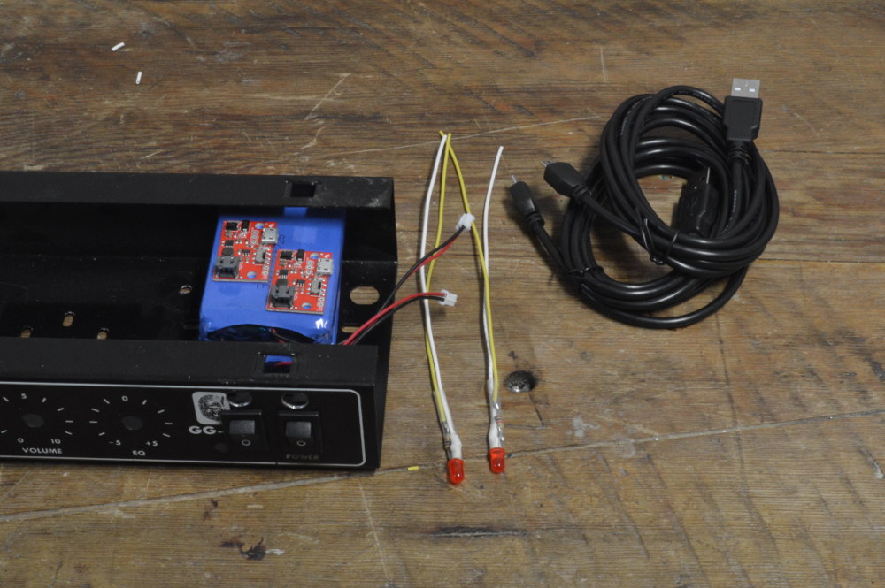
The switches are wired to the enable pin, so each switch can suspend the PAM2401 booster IC. Each booster has a hard-wired USB cable that will dangle within the amp. Two separate chargers are needed because the booster outputs are connected in series.
An unusual effect of this type of supply wiring is that either power supply can be used on its own for about 5V, or both can be used to deliver 10V. With a single supply off, current is bypassed through the booster's diode so no harm is done.
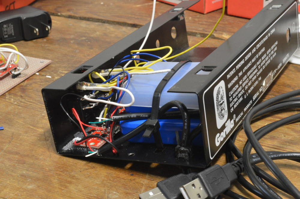
I found the batteries fit well where the transformer was mounted. To protect the packs from being pinched by the zip-ties, I cut a section from an old SIK case and placed it above the packs. The charger/boosters are hook-and-loop attached to the chassis so they can be removed in the dreadful case that something needs to be modified (it worked first try!).
The Results
I'm really happy with how well the electronics fit into the chassis. It leaves room for the other potentiometers to fit back in, and even some spare room for more circuits. The connecting wires are all soldered from the top, though, so changing the wiring after the fact isn't a problem.
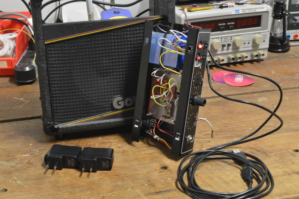
The amp draws about 200--300 milliamps with a single supply switched on, for about 24 hours of use per pack. And the volume is great for practice, or for playing with a small group.
There is a lot of noise I'm battling, though, which I've isolated to the PSoC. Have a listen to this MP3 to hear for yourself.
In the recording, the amp is turned up all the way. With no input signal, a scope measures a clean input to the ADC, but the PSoC debugger reveals about 10 counts of variation of the signal.
Are you an analog PSoC pro? Give me some tips if you've got them. Other questions or thoughts? Comment away!
Have a hacky holiday,
Marshall


