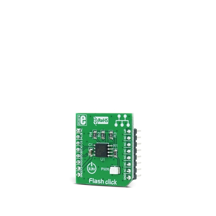
MIKROE Flash Click
MIKROE Flash Click is 8,388,608 bits (8 Mbit) on a Click board™, organized into 1,048,576 bytes (1 MB).
Product Overview
MIKROE Flash Click is 8,388,608 bits (8 Mbit) on a Click board™, organized into 1,048,576 bytes (1 MB). In other words, this Click board™ is a flash memory medium with the capacity of 1 MB. The used flash module has very good endurance and it can withstand up to 100,000 write cycles, with the data retention period of about 20 years. The flash memory IC used on this Click board™, features Serial Flash Discoverable Parameters (SFDP) mode, used to retrieve the advanced information from the device, such as the operating characteristics, structure and vendor specified information, memory size, operating voltage, timing information, and more.
Due to the high data transfer speed via the standard SPI interface, as well as the improved reliability of the stored information, this Click board™ can be used as a mass storage option in multimedia devices, data drives, non-volatile data storage in embedded applications, and similar applications that require reliable permanent storage of data blocks. Addition of 512 bytes of one-time programmable (OTP) memory can be useful for building secure storage devices and similar secure storage applications.
The flash memory module used on this Click board™ is the EN25Q80B, an 8 Mbit serial flash memory with 4 KB Uniform Sector, from EON Silicon Solutions. The flash memory density is usually expressed in bits, so exactly 8,388,608 bits are organized in units of 8 bits (bytes), which gives 1,048,576 bytes of data memory. This memory module contains 256 sectors of 4 KB, each, as well as 16 blocks of 64 KB, each. Furthermore, the memory is organized in pages. One page holds 256 bytes and there are 4096 pages (4096 pages x 256 bytes = 1,048,576 bytes total). Having insight into how the memory cells are organized, is very important for understanding the Write and Erase operations. The SPI pins are routed to the mikroBUS™ so the interfacing with the microcontroller unit (MCU) is easy and straightforward. The EN25Q80B communication consists of sending the instruction from the host MCU, followed by either an address, data, or both.
Before attempting any write operations to the flash memory, the Write Enable bit (WEL) of the Status Register needs to be set to 1. This bit is automatically set to 0 after some instructions, as well as during the Write operation itself, preventing accidental damage to the memory content. There are special instructions used to set and clear the WEN bit of the Status Register. Usually, every write operation will be prefixed with the WREN instruction.
Page Program instruction allows up to 256 bytes to be written during one write cycle. After the initial command, three more address bytes are sent, followed by the data that needs to be written. It is possible to write less than 256 bytes, which will be written at the starting address, not affecting the rest of the data on the same page. After successful write cycle, the state of the Write in Progress (WIP) bit is set to 0 automatically, and the device is ready to accept another erase or write instruction. Therefore, the status register can be polled for the status of the WIP bit, in order to shorten the wait time for the next operation.
Data can be read by the Read Data Bytes instruction. This instruction is followed by an address, from which the data is shifted to the output register and read by the host MCU. The address increment is automatically executed, making it possible to read the entire memory by a single Read Data command. HIGH logic level on the chip select pin (CS) will terminate the operation.
An interesting fact is that Page Program instruction can only reset the bits to 0. Therefore, a segment of memory needs to be erased prior to programming, or in this case - filled with 1s (0xFF). The EN25Q80B IC allows erasure of one sector at a time (Sector Erase instruction, 0x20), half a block at a time (Half Block Erase instruction, 0x52), block at a time (Block Erase instruction, 0xD8), and the entire memory (using the Chip Erase instruction, 0x60). The same mechanism applies here too: polling the WIP bit helps to shorten the wait for the total time for the next operation.
A dedicated #WP write protect pin is used to put the device into the hardware write protect mode. This pin is routed to the RST pin of the mikroBUS™. A LOW logic level on this pin allows locking down of the Block Protect bits and the Status Register Protect (SRP) bit. Locking down the Status Register will block changes of the WEN bit, which is required for the Write and Erase operations, effectively preventing the memory content changes. The Write Protect disable (WPDIS) non-volatile bit is used to control the function of the #WP pin: if set to 1, the #WP pin function is disabled.
Besides working in SPI mode, the EN25Q80B IC is capable of working in Dual SPI and Quad SPI modes. There are special Dual and Quad SPI instructions, which utilize these two additional modes, allowing several times faster data transfer speeds. When using Quad SPI instructions, the SDI and SDO pins become DQ0 and DQ1, while the WP and HLD pins become DQ2 and DQ3, respectively. All other operations use the standard SPI interface with single output signal. Due to a small number of MCUs that support Dual and Quad SPI, MikroElektronika offers library functions which work only with the standard SPI communication, ensuring the absolute compatibility with all the supported MCUs.
There are 512 bytes of OTP memory, which can be used to store various security data. Once programmed, this memory can be permanently locked, without a possibility to reprogram it ever again. This feature utilizes the OTP_LOCK bit. Until this bit is 0, the OTP memory block can be freely programmed, just like any other block. When this bit is set to 1, this block won’t be programmable anymore. Once set, the OTP_LOCK bit cannot be reset.
EN25Q80B features Serial Flash Discoverable Parameters (SFDP) mode. Host MCU can retrieve the operating characteristics, structure and vendor specified information such as identifying information, memory size, operating voltage and timing information of this device by sending the SFDP Read command (0x5A), followed by 3 bytes of address and one dummy byte. This will initiate a cyclic transfer from the SFDP memory table, which can be stopped at any moment by driving the chip select pin (CS) to a HIGH logic level.
For the detailed commands explanation and more in-depth information, please consult the included datasheet. However, MikroElektronika provides a library which contains functions that simplify and speed up working with this device. The provided application example demonstrates the functionality of the library functions. It can be used as a reference for a custom project development.


Features & Specs
- Interface: SPI
- Compatibility: mikroBUS™
- Dimensions: 28.6 x 25.4mm
- Input Voltage: 3.3V
Documentation
Customer Reviews

Stock and Customer Discounts
Available Discounts
- $9.45 | 25+ units
- $8.96 | 100+ units