MIKROE Semper Flash Click
MIKROE Semper Flash Click is a Click board™ which features the S25HS512T, a perfect solution for the mass storage option in various embedded applications.
Product Overview
The Semper Flash Click is a Click board™ which features the S25HS512T, a perfect solution for the mass storage option in various embedded applications. With fast performance being one of its key features, Semper Flash Click can also be used for the code shadowing, execute-in-place (XIP), data logging and data storage. The Cypress Semper Flash with Quad SPI family of products are high-speed CMOS, MirrorBit NOR flash devices. Semper Flash is designed for Functional Safety with development according to ISO 26262 standard to achieve ASIL-B compliance and ASIL-D readiness. Built-in Error Correcting Code (ECC) corrects Single-bit Error and detects Double-bit Error (SECDED) on memory array data. The 512 Mbit SPI Flash memory module is one of the fastest and most reliable Flash modules on the market.
The Semper Flash Click is supported by a mikroSDK compliant library, which includes functions that simplify software development.
The Semper Flash Click is memory module based on the S25HS512T a 512 Mbit SPI Flash memory module, from Cypress. Featuring both normal and double data rates over the standard, Dual/Quad SPI interface, the improved reliability of the stored information by utilizing the hardware Error Correction Code (ECC) generation, One-Time Programmable (OTP) memory block of 1024 bytes, an advanced sector protection, AutoBoot, and much more, this Click board™ is a perfect solution for the mass storage option in various embedded applications. Due to its fast performance, Semper Flash Click can also be used for the code shadowing, execute-in-place (XIP), data logging and data storage. An additional level translator IC allows Semper Flash Click to be used with a wide range of MCUs.
The device control logic is subdivided into two parallel operating sections: the Host Interface Controller (HIC) and the Embedded Algorithm Controller (EAC). The HIC monitors signal levels on the device inputs and drives outputs as needed to complete read, program and write data transfers with the host system. The HIC delivers data from the currently entered address map on read transfers; places write transfer address and data information into the EAC command memory, and notifies the EAC of power transition, and write transfers. The EAC interrogates the command memory, after a program or write transfer, for legal command sequences and performs the related Embedded Algorithms.
Executing code directly from Flash memory is often called Execute-In-Place (XIP). By using XIP with Semper Flash devices at the higher clock rates with Quad or DDR Quad SPI transactions, the data transfer rate can match or exceed traditional parallel or asynchronous NOR flash memories while reducing signal count dramatically.
The advanced MirrorBit® technology allows storing of two data bits in each memory array transistor (memory cell), effectively doubling the capacity of a single storage cell this way. The Eclipse™ architecture is responsible for the greatly improved erase and programming performance, compared to other Flash modules of the previous generation. Due to a higher speed, an execute-in-place (XIP), as well as the data shadowing is possible with the Semper Flash Click.
One of the key features of the S25HS512T is certainly the AutoBoot feature. It allows the module to automatically initiate the memory transfer from the predefined location (memory read operation) after the reset cycle. Considering a typical communication scenario, where READ command followed by the one or more address bytes need be used, AutoBoot allows the host MCU to pull down the #CS (Chip Select) pin and start receiving a data stream over the SPI interface for as long as the #CS pin is held LOW, without any wasted cycles. As soon as the #CS pin is released, the S25HS512T returns to a normal operation.
The Advanced Sector Protection (ASP) is a powerful protection model that incorporates a set of various software and hardware methods to enable or disable programming or erase operations within a sector or an entire memory. A specialized ASP OTP register offers a password protection mode or a persistent protection mode, allowing an increased flexibility of the protection. Using the OTP memory allows the protection mode to remain in place for the whole life-cycle of the device.
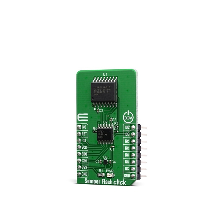
The SPI interface pins are routed to the mikroBUS™ so that the interfacing with the microcontroller unit (MCU) is easy and straightforward. Additional pins routed to the mikroBUS™ include the #WP/IO2 pin routed to the mikroBUS™ PWM pin and labeled as IO2, and #HOLD/IO3 pin routed to the mikroBUS™ INT pin and labeled as IO3. There is also the RESET pin, routed to the RST pin of the mikroBUS™, which performs a reset of the Flash module, initiating an AutoBoot sequence if enabled.
EnduraFlex Architecture provides system designers the ability to customize the NOR Flash endurance and retention for their specific application. The host defines partitions for high endurance or long retention, providing up to 1+ million cycles or 25 years of data retention.
Data Integrity Check transactions in Semper Flash perform a hardware accelerated Cyclic Redundancy Check (CRC) calculation over a user defined address range in the memory array. The SafeBoot feature allows Status Register polling to detect an embedded microcontroller initialization failure or configuration register corruption through error signatures.
Features & Specs
- Interface: QSPI, SPI
- Compatibility: mikroBUS™
- Dimensions: 42.9 x 25.4mm
- Input Voltage: 3.3V
- Memory Size: 512 Mbit
Documentation
Customer Reviews

Stock and Customer Discounts
Available Discounts
- $23.70 | 25+ units
- $22.46 | 100+ units