MIKROE DAQ Click
MIKROE DAQ Click is a compact add-on board representing a data acquisition solution.
Product Overview
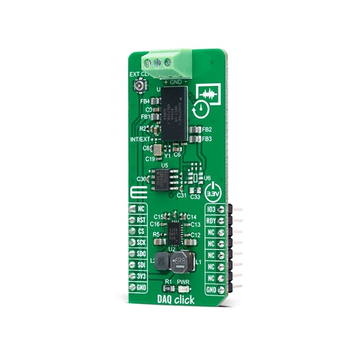
MIKROE DAQ Click is a compact add-on board representing a data acquisition solution. This board features the ADAQ7768-1, a 24-bit precision data acquisition (DAQ) μModule system that encapsulates signal conditioning, conversion, and processing blocks into one SiP from Analog Devices. It supports a fully differential input signal with a maximum voltage range of ±12V with an excellent common-mode rejection ratio (CMRR). The input signal is fully buffered with a low input bias current, enabling the ADAQ7768-1 to interface to sensors with high output impedance directly. Also, it comes with a selectable clock source and programmable gain options, output data rate, filter type, and latency configurable through an SPI serial interface. This Click board™ is suitable as a universal input measurement platform for electrical tests and measurements, condition monitoring for predictive maintenance, and many other applications.
DAQ Click is supported by a mikroSDK compliant library, which includes functions that simplify software development.
DAQ Click as its foundation uses the ADAQ7768-1, a 24-bit precision data acquisition μModule system that encapsulates signal conditioning, conversion, and processing blocks into one SiP from Analog Devices, enabling rapid development of highly compact, high-performance precision DAQ systems. The ADAQ7768-1 consists of low noise, high bandwidth programmable gain instrumentation amplifier (PGIA) capable of signal amplification and attenuation while maintaining high input impedance. Also, it has a linear phase anti-aliasing filter, a high-performance 24-bit sigma-delta ADC with a programmable digital filter, a low dropout linear regulator, and reference buffers, alongside critical passive components required for the signal chain.
The wide common-mode input range of the ADAQ7768-1 allows it to accept a wide variety of signal swings. It supports a fully differential input signal connection with a maximum voltage range of ±12V with an excellent common-mode rejection ratio. The input signal is fully buffered with a low input bias current, enabling the ADAQ7768-1 to interface to sensors with high output impedance directly. The ADAQ7768-1‘s PGA requires a voltage of ±15V to supply the frontend amplifiers. Therefore, a dual-channel low-noise bias generator, the LT3095 from Analog Devices, provides a +15V out of 3V3 mikroBUS™ rail, while a -15V supply is obtained by combining a step-down regulator ADP2300 and a small low-noise LDO ADP7182, both from Analog Devices, also out of 3V3 mikroBUS™ rail. The PGIA has six gain settings capable of varying input ranges from ±0.197V to ±12.603V fully differential input signal, which can be configured with GAIN pins controlled by three multifunction GPIO pins of the ADAQ7768-1 (MODE1-3).
An integrated 4th order low-pass analog filter combined with the user-programmable digital filter ensures the signal chain is fully protected against the high-frequency noise and out-of-band tones presented at the input node. This filter is designed to achieve high phase linearity and maximum in-band magnitude response flatness. Inside the ADAQ7768-1, there is also a high-performance, 24-bit precision, single-channel Sigma-Delta converter with excellent AC performance and DC precision, and throughput rate of 256kSPS from a 16.384MHz onboard crystal (clock source). In addition to the internal clock source, the user can also use an external clock brought to the connector labeled as EXT CLK. Selection of the clock source is performed by positioning a jumper marked as INT/EXT.
Since the LT3095 generates two independent supplies, in addition to -15V, this regulator also provides the 5.3V voltage required to power the internal LDO of the ADAQ7768-1, whose output supplies an onboard voltage reference the ADR4540. This Click board™ also allows the user to filter the reference voltage itself, with the optional use of a reference buffer implemented using OpAmp, ADA4807-1, which provides high-speed performance with a DC precision, low noise distortion, and power to maintain the accuracy of the reference.
This Click board™ communicates with MCU through a standard SPI interface to program the internal registers for complete control of the ADAQ7768-1. In addition, it uses several GPIO pins such as reset pin routed to the RST pin on the mikroBUS™ socket, which with a low logic level puts the module into a Reset state, an additional data-ready signal, routed on the INT pin of the mikroBUS™ socket labeled as RDY, indicating that new data is ready for the host, and one extra user-configurable general-purpose I/O pin labeled as IO3 routed to the PWM pin on the mikroBUS™ socket.
This Click board™ can be operated only with a 3.3V logic voltage level. The board must perform appropriate logic voltage level conversion before use with MCUs with different logic levels. However, the Click board™ comes equipped with a library containing functions and an example code that can be used, as a reference, for further development.

Features & Specs
- Interface: SPI
- Compatibility: mikroBUS™
- Dimensions: 57.15 x 25.4mm
- Input Voltage: 3.3V
- Maximum Input Voltage Range: Min. -12V, Max. 12V
- Gain Selection: Min. 0.325 V/V, Max. 20.8 V/V
- ADC Resolution: 24 bits
- External Clock Frequency Range: Min. 0.6MHz, Typ. 16.384MHz, Max. 17MHz
- Operating Temperature Range: Min. -40°C, Typ. +25°C, Max. +105°C
Customer Reviews

Stock and Customer Discounts
Available Discounts
- $71.20 | 25+ units
- $67.46 | 100+ units