MIKROE nvSRAM 2 Click
nvSRAM 2 Click is a compact add-on board that contains the most reliable nonvolatile memory.
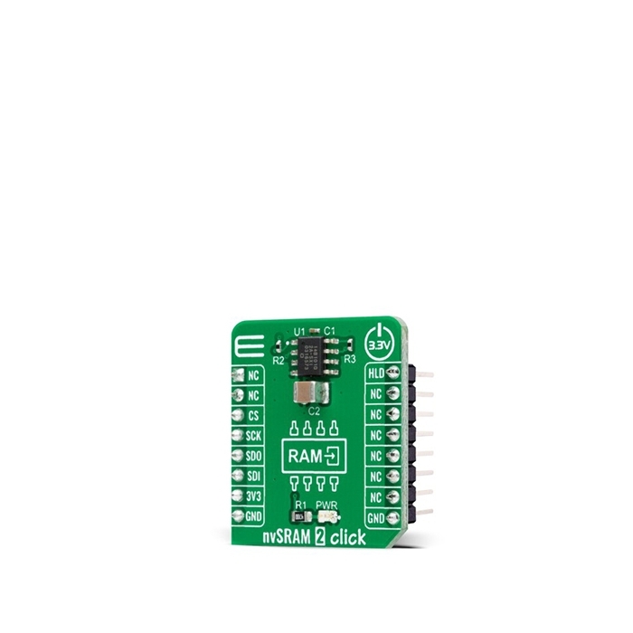
Product Overview
nvSRAM 2 Click is a compact add-on board that contains the most reliable nonvolatile memory. This board features the CY14B101Q, a 1Mbit nvSRAM organized as 128K words of 8 bits each with a nonvolatile element in each memory cell from Infineon. The embedded nonvolatile elements incorporate the QuantumTrap technology and provide highly reliable nonvolatile storage of data. Data transfer, initiated by the user through SPI commands, from SRAM to the nonvolatile elements takes place automatically at Power-Down. On the other hand, during the Power-Up, data is restored to the SRAM from the nonvolatile memory. This Click board™ is suitable for all applications that require fast access and high reliability of stored data, and unlimited endurance.
nvSRAM 2 Click is supported by a mikroSDK compliant library, which includes functions that simplify software development.
nvSRAM 2 Click is based on the CY14B101Q, a 1-Mbit nvSRAM organized as 128K words of 8 bits each with a nonvolatile element in each memory cell from Infineon. The nvSRAM specifies one million endurance cycles for nonvolatile cells with data retention of a minimum of 20 years. All the reads and writes to nvSRAM happen to the SRAM, which gives nvSRAM the unique capability to handle infinite writes to the memory. Besides, the benefit of nvSRAM over serial EEPROMs is that all reads and writes to nvSRAM are performed at the SPI speed with zero cycle delay. Therefore, no wait time is required after any of the memory accesses.
In the event of system power loss, data from the SRAM is transferred to its nonvolatile cell automatically by using energy stored in a capacitor labeled as C2. During the Power-Up, data from the nonvolatile cell is recalled automatically in the SRAM array and available to the user. The endurance cycle is consumed only when data transfer happens from the SRAM cells to nonvolatile cells during the Power-Down.
The memory can be accessed through a standard SPI interface that enables high clock speeds up to 40 MHz with zero cycle delay read and write cycles. It also supports the two most common modes, SPI Mode 0 and 3, and 104 MHz SPI access speed with special instruction for the read operation. The CY14B101Q uses the standard SPI opcodes for memory access. In addition to the general SPI instructions for reading and writing, it provides four special instructions: STORE, RECALL, AutoStore Disable (ASDISB), and AutoStore Enable (ASENB).
In addition to this, the nvSRAM 2 Click also has an additional HOLD pin, routed to the PWM pin of the mikroBUS™ socket labeled as HLD, used to pause the serial communication with the device without having to stop the operation of write status register, programming, or erasing in progress.
This Click board™ is designed to be operated only with a 3.3V logic voltage level. A proper logic voltage level conversion should be performed before the Click board™ is used with MCUs with different logic levels.


Features & Specs
- Interface: SPI
- Compatibility: mikroBUS™
- Dimensions: 28.6 x 25.4mm
- Input Voltage: 3.3V
- Supply Voltage: Min. -0.5V, Typ. 3.3V, Max. 4.1V
- Memory Size: 1 Mbit
- nvSRAM Write Endurance: 1.000.000 Write Cycles
- nvSRAM Data Retention: 20 Years
- Operating Temperature Range: Min. -40°C, Max. +85°C
Documentation
Customer Reviews

Stock and Customer Discounts
Available Discounts
- $28.45 | 25+ units
- $26.96 | 100+ units