
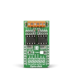
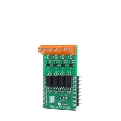
MIKROE Opto 2 Click
Opto 2 Click uses four TLP2770, 20Mbps low-power optocouplers, from Toshiba.
Product Overview
Opto 2 Click is a galvanic isolator Click board™, used to provide an optical isolation of sensitive microcontroller (MCU) pins, when operated by external signals. TLP2770 opto-isolation elements (optocouplers) can be driven with a very low current, down to 1.3mA (min). A choice of high-speed optocouplers allows Opto 2 Click to be used on communication lines, with up to 20 Mbps data rates. This Click board™ can be used to provide an optical isolation when there is a requirement for a high reinforced isolation between the external signal lines and the controller logic with a MCU such as in PLCs or similar applications.
Opto Click 2 can be used in applications where the MCU input side is under risk of high voltage surges in a noisy environment. Since it provides a galvanic isolation, the electrical potential of the input side circuit does not have to be the same as the electrical potential of the MCU circuit. Featuring a reinforced galvanic isolation, Opto 2 Click blocks so-called stray currents, that may appear as a result of differences in ground potential, or the electromagnetic induction. Opto 2 Click provides means to drive inputs of the connected MCU with a wide range of external applications and signals.
Opto 2 Click uses four TLP2770, 20Mbps low-power optocouplers, from Toshiba. These are fast optocouplers, with their output stages shielded against EMI, allowing them to work on higher speeds, providing common-mode transient immunity of ±20 kV/μs. The internal LED elements are driven with 4mA for 5V operation or 2.6mA for 3.3V operation. The input stages are also equipped with (Schottky) diodes, which prevents inverse polarization of the LED elements and thus, a permanent damage that might occur in that case.
The working principle of the optocouplers is quite simple: A photo-emitting element - usually a LED, is encapsulated inside the die along with the photo-sensitive element, which can be a photo-sensitive transistor or a photo-diode. LEDs and photo-sensing elements are galvanically isolated, making the input and output electrical networks completely independent of each other. When the LED is biased, it emits light which in return causes the current to flow through the photo-sensitive element. In these particular optocouplers, the output stage is additionally conditioned by a Schmitt trigger and it drives the output transistors which form a totem pole output stage. Having a totem pole output configuration allows the output stage to both sink and source current.
The optocoupler inputs - the anodes (labeled as A) and cathodes (labeled as C) of the internal optocoupler LEDs, are routed to the screw terminals, which allow connection the external electrical circuit, used to trigger an event on the isolated MCU. The electrical potential between the anode and the cathode input of each optocoupler element should stay within the range between 3.3V and 5V.
The optocoupler outputs are routed to the mikroBUS™ The mikroBUS™ pins INT, CS, RST, and AN, are routed to the optocoupler outputs 1, 2, 3, and 4, respectively, and are labeled as IN1, IN2, IN3, and IN4. As already mentioned, the output stages are conditioned with the Schmitt trigger circuit, reducing the input noise sensitivity and false triggering. The Faraday shield protects the output stages against EMI and provides common-mode transient immunity of ±20 kV/μs. Although these mikroBUS™ pins are labeled as IN1 to IN4, they are actually outputs from the optocouplers, and it is highly recommended to use them as the INPUT pins on the host MCU.
The Click board™ is equipped with an SMD jumper labeled as LOGIC, which allows selection of the voltage, applied to the optocoupler output stage. This voltage effectively determines the logic voltage level for the MCU pins. It can be selected between 3.3V and 5V, allowing this Click board™ to be interfaced with both 3.3V and 5V MCUs.
The provided library offers functions that simplify and speed up the application development. The included example application demonstrates their use. This application can be used as a reference for custom projects.
Features & Specs
- Interface: GPIO
- Compatibility: mikroBUS™
- Dimensions: 42.9 x 25.4mm
- Input Voltage: 3.3V or 5V
- Input Forward Current (IF): 8mA
- Peak Transient Input Forward Current (IFPT): 1A
- Output Current (IO): 10mA
Documentation
Customer Reviews
Stock and Customer Discounts
Available Discounts
- $23.70 | 25+ units
- $22.46 | 100+ units