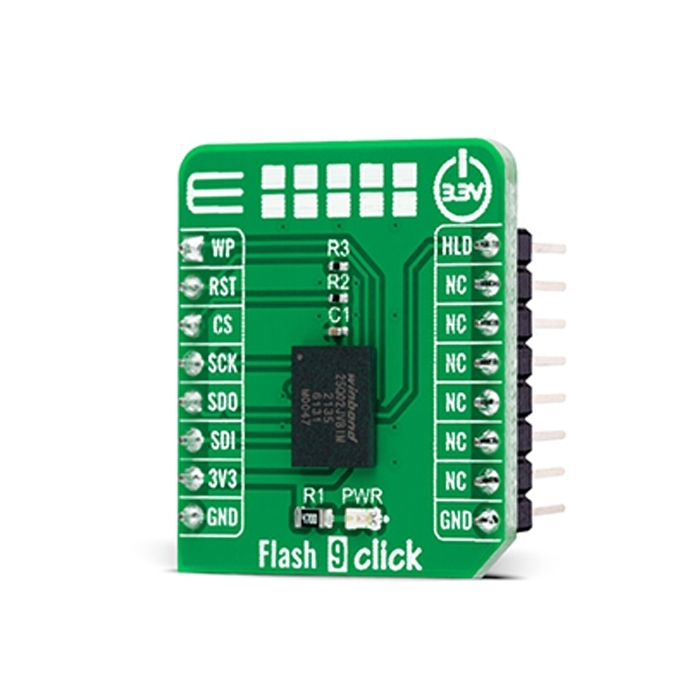
MIKROE Flash 9 Click
Flash 9 Click is a compact add-on board that contains a highly reliable memory solution.
Product Overview
Flash 9 Click is a compact add-on board that contains a highly reliable memory solution. This board features the W25Q02JV, an SPI configurable serial Flash memory solution from Winbond Electronics. It represents a four 512Mb stack die supporting linear addressing for the full 2Gb memory address range, offering flexibility and performance well beyond ordinary Serial Flash devices. The W25Q02JV array is organized into 1,048,576 programmable pages of 256-bytes each, where up to 256 bytes can be programmed at a time. This memory also has advanced security features, can withstand many write cycles (minimum 100k), and has a data retention period greater than 20 years. This Click board™ provides a storage solution for limited space and power systems in various embedded applications.
Flash 9 Click is supported by a mikroSDK compliant library, which includes functions that simplify software development.
Flash 9 Click as its foundation uses the W25Q02JV, a highly reliable serial Flash memory solution offering flexibility and performance well beyond ordinary Serial Flash devices from Winbond Electronics. The W25Q02JV represents a four 512Mb stack die where only one can be active at any given time to communicate with the external SPI controller. It supports linear addressing for the full 2Gb memory address range (continuously-read accessible only into four separate 512Mb address memory segments). The W25Q02JV array is organized into 1,048,576 programmable pages of 256-bytes each, where up to 256 bytes can be programmed at a time.
Pages of the W25Q02JV can be erased in groups of 16 (4KB sector erase), groups of 128 (32KB block erase), groups of 256 (64KB block erase), or the entire chip (chip erase). This IC has 32,768 erasable 4KB sectors and 2,048 erasable 64KB blocks, respectively. The small 4KB sectors allow for greater flexibility in applications that require data and parameter storage. Also, it specifies a minimum of 100.000 endurance cycles with data retention of a minimum of 20 years, which gives the W25Q02JV the capability to handle unlimited reads/writes to the memory.
Flash 9 Click communicates with MCU through a standard SPI interface that enables high clock speed, supporting the two most common SPI modes, SPI Mode 0 and 3. Alongside the internal software Reset sequence, this board also has an active-low reset signal routed on the RST pin of the mikroBUS™ socket used to reset the W25Q02JV to the initial power-on state. When this signal is asserted low, any ongoing program/erase operation will be interrupted, and data corruption may happen (the device will not accept any command input).
An additional feature of this Click board™ represents the configurable Write Protection function labeled as WP routed on the AN pin of the mikroBUS™ socket. The WP pin protects the entire memory and all registers from write operations and must be set to a low logic state to inhibit all the write operations. Besides, the Flash 9 Click also has an additional hold pin, labeled as HLD and routed to the PWM pin of the mikroBUS™ socket, allowing the device to be paused while it’s still actively selected.
This Click board™ can be operated only with a 3.3V logic voltage level. The board must perform appropriate logic voltage level conversion before using MCUs with different logic levels. However, the Click board™ comes equipped with a library containing functions and an example code that can be used, as a reference, for further development.
Features & Specs
- Interface: SPI
- Compatibility: mikroBUS™
- Dimensions: 28.6 x 25.4mm
- Input Voltage: 3.3V
- Memory Size: 2 Gbit
- Write Endurance: 100,000 cycles
- Data Retention: 20 years
- Operating Temperature Range: Min. -40°C, Typ. +25°C, Max. +85°C
Documentation
Customer Reviews

Stock and Customer Discounts
Available Discounts
- $56.95 | 25+ units
- $53.96 | 100+ units


