MIKROE FRAM 5 Click
FRAM 5 Click is a compact add-on board representing a highly reliable ferroelectric random access memory solution.
Product Overview
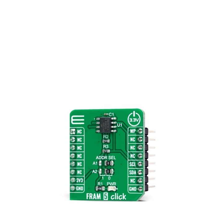
FRAM 5 Click is a compact add-on board representing a highly reliable ferroelectric random access memory solution. This board features the FM24V10, a 1Mbit nonvolatile memory employing an advanced ferroelectric process organized as 128K words of 8 bits each from Infineon. This I2C configurable FRAM performs read and write operations similar to a RAM providing reliable data retention for 151 years while eliminating the complexities, overhead, and system-level reliability problems caused by EEPROM and other nonvolatile memories. This Click board™ is ideal for nonvolatile memory applications requiring frequent or rapid writes and unlimited endurance.
FRAM 5 Click is supported by a mikroSDK compliant library, which includes functions that simplify software development.
FRAM 5 Click as its foundation uses the FM24V10, a 1Mbit ferroelectric random access memory (FRAM) logically organized as 131,072×8 bits and accessed using an industry-standard I2C interface from Infineon. The functional operation of the FRAM is similar to serial I2C EEPROM, where the significant difference between the FM24V10 and EEPROM represents the F-RAM's superior write performance, high endurance, and low power consumption. This Click board™ is ideal for nonvolatile memory applications requiring frequent or rapid writes, where example ranges from data collection to demanding industrial controls where the long write time of serial EEPROM can cause data loss.
This Click board™ communicates with MCU using the standard I2C 2-Wire interface, supporting operation with a clock frequency up to 3.4MHz. Unlike serial EEPROM, the FM24V10 performs write operations at bus speed, where no write delays are incurred. It provides reliable data retention for 151 years while eliminating the complexities, overhead, and system-level reliability problems caused by EEPROM and other nonvolatile memories and supports 10 trillion (1014) read/write cycles or 100 million times more write cycles than EEPROM. Besides, the FM24V10 allows choosing its I2C peripheral address using the SMD jumpers labeled ADDR SEL. The selection can be made by positioning the SMD jumpers to an appropriate position marked as 1 or 0.
An additional feature of this FRAM represents the configurable Write Protection function labeled as WP routed on the PWM pin of the mikroBUS™ socket. The WP pin protects the entire memory and all registers from write operations and must be set to a high logic state to inhibit all the write operations. All memory and register writes are prohibited when this pin is high, and the address counter is not incremented.
This Click board™ can be operated only with a 3.3V logic voltage level. The board must perform appropriate logic voltage level conversion before using MCUs with different logic levels. However, the Click board™ comes equipped with a library containing functions and an example code that can be used, as a reference, for further development.


Features & Specs
- Interface: I2C
- Compatibility: mikroBUS™
- Dimensions: 28.6 x 25.4mm
- Input Voltage: 3.3V
- Memory Size: 1 Mbit
- Write Endurance: 1014 Write Cycles
- Data Retention: 151 Years
- Operating Temperature Range: Min. -40°C, Typ. +25°C, Max. +85°C
Documentation
Customer Reviews

Stock and Customer Discounts
Available Discounts
- $37.95 | 25+ units
- $35.96 | 100+ units