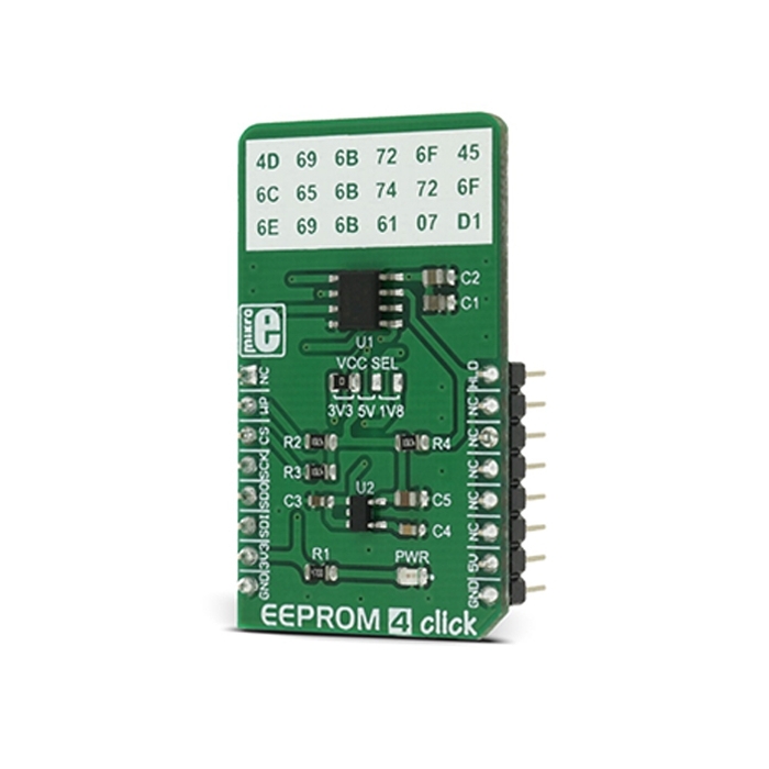
MIKROE EEPROM 4 Click
The EEPROM module used on the EEPROM 4 Click is the AT25M02, an SPI serial EEPROM from Microchip, with the memory cell density of 2 Mbits.
Product Overview
EEPROM 4 Click is 2,097,152 bits on a Click board™, organized into 262,144 bytes. In other words, this Click board™ is an EEPROM memory medium with the capacity of 256 KB. The used EEPROM module has very good endurance and it can withstand 1,000,000 write cycles, with the data retaining period of about 40 years. The EEPROM module on this Click can work with power supply voltage ranging from 1.7V to 5.5V, it features the self-timed write cycles, doesn’t require erase before writing, has a dedicated write protect pin for hardware protection of stored data, and has a dedicated hold pin used for holding the data transfer.
EEPROM 4 Click is aimed towards industrial and commercial applications, which require low voltage and low power operational capabilities. It can be used for any kind of temporary or permanent data storage for various embedded electronic devices, simple data logging, storing various working parameters of a module or device, safeguarding the sensitive data in case of a power cycle, and other similar applications where EEPROM memory is needed.
The EEPROM module used on the EEPROM 4 Click is the AT25M02, an SPI serial EEPROM from Microchip, with the memory cell density of 2 Mbits. The EEPROM density is usually expressed in bits, so exactly 2,097,152 bits are organized in units or words of 8 bits, which gives 262,144 bytes of data memory. Furthermore, the EEPROM is organized in so-called pages. One page holds 256 bytes and there are 1024 pages (1024 pages x 256 bytes = 262,144 bytes total). Having insight into how the memory cells are organized, is important for write and erase operations. The SPI pins are routed to the mikroBUS™ so the communication is easy and straightforward. The SPI can be clocked as high as 5 MHz, providing a fast throughput for the data transfer.
Some other EEPROM memory modules require erasing of the whole memory page before writing new data. This EEPROM doesn’t require such operations. It features byte write and page write modes. Before attempting any write operations to the EEPROM, the write enable bit (WEL) of the Status Register needs to be set to 1. This bit is automatically set to 0 after some instructions. There are special instructions used to set and clear the WEN bit of the Status Register. These instructions are WREN (06h) and WRDI (04h). Usually, every write instruction will be prefixed with the WREN instruction.
- When using a Byte write instruction, one single byte will be written during the write cycle. After successful write cycle, the state of the WEL bit is set to 0 automatically and the device is ready to accept another byte to be written.
- When using a Page write instruction, 256 bytes will be written during one write cycle. It is possible to write less than 256 bytes, but if there is still incoming data when the end of the page is reached, the write pointer will roll over to the beginning of the same page, overwriting the content there. The special care should be taken to the page alignment. After successful write cycle, the state of the WEL bit is set to 0 automatically and the device is ready to accept another page of data to be written.
A dedicated #HOLD pin is routed to the PWM pin of the mikroBUS™. When the communication with the Click board™ is initiated by setting the CS pin to a LOW logic state, it is possible to pause the serial data transfer without resetting the communication, if the #HOLD pin (PWM pin on the mikroBUS™) is set to a LOW logic state. To resume the communication, it is enough to set this pin to a HIGH logic state while the SCK is still running. Once the HOLD is initiated, the state of the SCK line is irrelevant and any serial data input will be ignored. This pin is pulled HIGH by the onboard resistor.
A dedicated #WP write protect pin is used to put the device into the hardware write protect mode. This pin is routed to the RST pin of the mikroBUS™. Hardware write protect works in conjunction with the Write Protect Enable (WPEN) bit of the Status Register. When this bit is set to 1 and the #WP pin is set to a LOW logic state, the device will ignore any attempt to write to the Status Register and the EEPROM memory regions, selected by the Block Write Protect bits of the Status Register (BP0 and BP1). WRSR instruction is used to write to the Status Register (01h). Again, before attempting to write to Status Register, WREN instruction should be executed first. Once the WPEN bit is set to 1 and the RST has been pulled to a LOW logic state, setting the WPEN bit to 0, won’t disable write protection, as long as the #WP pin (RST) stays LOW. WPEN bit, as well as the BP0 and BP1 bits, are constructed as EEPROM cells, meaning that they are nonvolatile and will retain their states even after power off. The #WP pin is pulled HIGH by the onboard resistor.
The onboard SMD jumper labeled as VCCSEL is used to select the operating voltage between 3.3V and 5V, as usual. However, there’s the third position for this jumper, which is used to set the operating voltage to 1.8V. This is achieved thanks to the TC1015, a small 100 mA LDO from Microchip, which is powered from the 5V rail.
As always, MikroElektronika provides libraries that simplify and speed up working with this device. The provided application example demonstrates the functionality of the provided libraries and can be used as the reference point for own development.


Features & Specs
- Interface: GPIO, SPI
- Compatibility: mikroBUS™
- Dimensions: 42.9 x 25.4mm
- Input Voltage: 3.3V or 5V
Documentation
Customer Reviews

Stock and Customer Discounts
Available Discounts
- $14.20 | 25+ units
- $13.46 | 100+ units