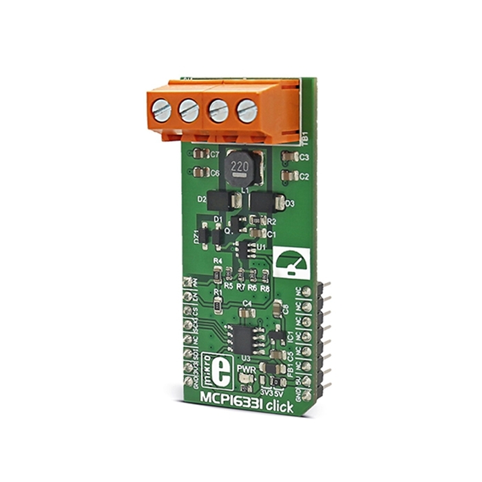
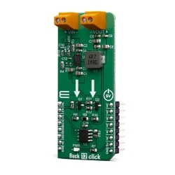
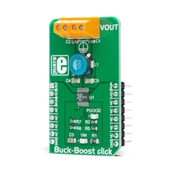
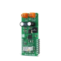
MIKROE MCP16331 Click
MCP16331 Click functions as a buck-boost voltage regulator.
Product Overview
MCP16331 Click functions as a buck-boost voltage regulator, a switching regulator topology that combines principles of the buck conversion (step-down) and the boost conversion (step-up).
A buck converter outputs voltage that is smaller than the input voltage (steps down the input voltage). A boost converter outputs voltage that is greater than the input voltage (steps up the input voltage).
By combining these two topologies, MCP16331 Click is able to output a regulated DC voltage, which can be set in the code, for input voltage both greater and less than the output voltage.
A typical application for a buck-boost regulator is a battery-powered system, where the input voltage can vary widely, starting at full charge and gradually decreasing as the battery charge is used up. At full charge, where the battery voltage may be higher than needed by the circuit, a buck regulator would be ideal to keep the supply voltage steady.
However as the charge diminishes the input voltage falls below the level required by the circuit, and either the battery must be discarded or re-charged; at this point, the ideal alternative would be the boost regulator.
By combining these two topologies, it is possible to have a regulator circuit that can cope with a wide range of input voltages both higher or lower than that required by the circuit.
This Click board™ central module is the Microchip's MCP16331, a non-synchronous, step-down or buck converter, capable of stepping input voltages ranging from 4.4V to 50V, and output voltage ranging from to 2.0V to 24V. More details about the MCP16331 are available in the official datasheet. However, MCP16331 Click is designed to handle an input voltage ranging from 4.5V to 18V and output a voltage ranging from 2,25V to 12V at 500 mA maximum current, since it works in a buck-boost topology.
To set the output voltage of the MCP16331 Click, the MCP4921 - a low power 12-Bit dual voltage output DAC is used in the feedback loop. The output of this DAC is used to drive the FB pin of the MCP16331, so in order to set up the output voltage, it is enough to set the DAC output to a specific value. This will cause the FB pin to drive the switching section of the MCP16331 which will output a desired voltage level, as a result. The AN pin of the mikroBUS™ can be used to verify the output voltage and correct the value given to the DAC, if needed. The MCP4291 DAC can be configured by the host MCU via the SPI bus pins, routed to the mikroBUS™.
The AN pin of the mikroBUS™ is routed to a middle point of a voltage divider on the output. This voltage divider is used to scale down the output voltage so it can be successfully converted by the ADC of the host MCU. Besides the bit depth of the ADC, this should also be taken into account when calculating the value for the output voltage.
The MCP16331 Click has two screw terminals used to connect the input voltage and the load, as well as the SMD jumper used to select the voltage for the DAC IC. This affects the SPI logic voltage levels, so both 3.3V and 5V MCUs can be used with this Click board™
NOTE: To avoid any possible damage to any load connected to the VOUT terminal, you must follow the correct power-up sequence:
- Disable the MCP16331 by setting the mikroBUS™ pin RST (EN) low (GND)
- Set the desired output voltage via SPI (see the software section below)
- Enable the MCP16331 by setting the mikroBUS™ pin RST (EN) high (5V)
The reason for this sequence is that the enable pin (EN) of the MCP16331 has an internal pull-up resistor that keeps the MCP16331 output stage enabled even if the pin is left unconnected. At power-up, before you set the voltage via SPI, DAC output is unspecified and the output voltage may set higher than what your load supports.
Libraries, provided with the MCP16331 Click will allow for simple and effortless setup of the necessary parameters. The included demo application can be used as a reference for future designs, and it demonstrates the functionality of the Click board™, as well as the included software libraries.

Features & Specs
- Interface: SPI
- Compatibility: mikroBUS™
- Dimensions: 57.15 x 25.4mm
- Input Voltage: 3.3V or 5V
- Input Voltage Range (VIN): Min. 4.5V, Max. 18V
- Output Voltage Range (VOUT): Min. 2.25V, Max. 12V
- Output Current: 500 mA
- Switching Frequency: 500 kHz
- Efficiency: 96%
Documentation
Customer Reviews
Stock and Customer Discounts
Available Discounts
- $20.85 | 25+ units
- $19.76 | 100+ units