MIKROE FRAM Click
MIKROE FRAM Click is a Click board™ that carries a ferroelectric RAM module.
Product Overview
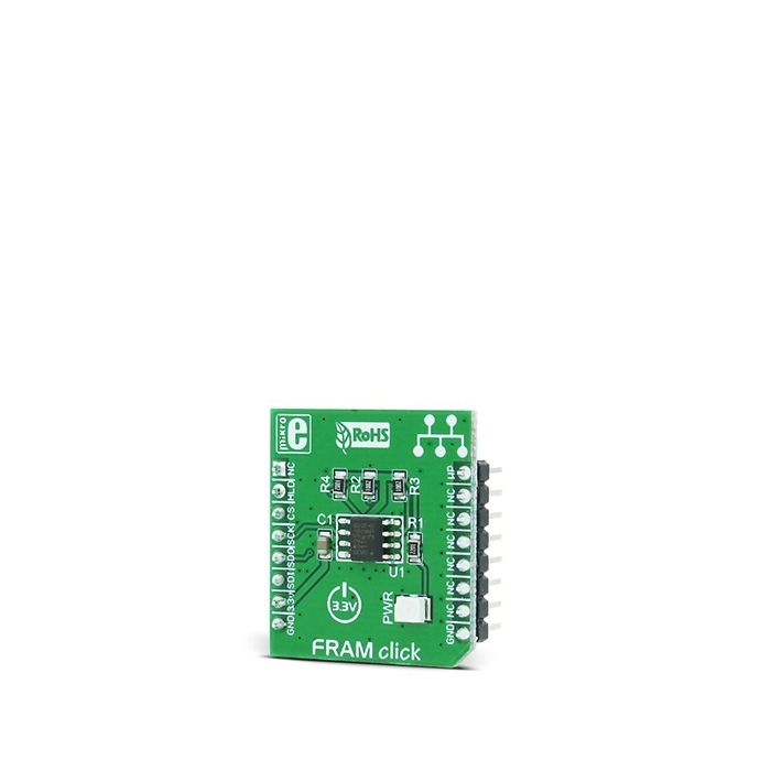
MIKROE FRAM Click is a Click board™ that carries a ferroelectric RAM module. Ferroelectric RAM, also known as FRAM, is a non-volatile memory type, with characteristics comparable to much faster DRAM memory modules. It offers much faster alternative to common serial FLASH and EEPROM modules, which use the conventional technologies. FRAM click uses the MB85RS256A, a 256 Kbit serial FRAM module from Fujitsu Semiconductor LTD. Although the FRAM is still being developed, this company managed to provide a very reliable and fast FRAM module that can write data at bus speed, has an extremely high endurance of 1010 read/write cycles, data retention period of 10 years, and very fast SPI interface.
Besides the unique technology used for the data storage, this device kept the backward compatibility, in sense of communication and operation. Offering these advanced features, as well as a range of standard features found on most EEPROM or FLASH modules, the FRAM click is ideal for nonvolatile memory applications, requiring frequent or rapid writes. It can be used for a wide range of applications, from data collection, where the number of write cycles may be critical, to demanding industrial controls, where the long write time of serial FLASH or EEPROM memory modules can cause data loss.
FRAM click is equipped with the MB85RS256A, a 256 Kbit serial ferroelectric (FRAM) module from Fujitsu Semiconductor LTD. It contains 262,144 bits of memory, organized in 32,768 byes. This means that the storage area contains 32 KB of address space. This memory IC is manufactured using the ferroelectric technology, which has many advantages over the conventional technologies used for manufacturing EEPROM and FLASH memory modules.
Ferroelectric technology is still being developed and perfected, but the advantages have already been demonstrated. This technology exploits the properties of ferroelectric materials to retain the electric field after they have been exposed to it, the same way the ferromagnetic materials retain their magnetic field. This phenomenon is employed to polarize the FRAM cells and store the information. One of the areas that still need to be improved is the thermal instability, especially on high temperatures. When the ferroelectric material reaches the Curie temperature, its properties are degraded.
Therefore, the high temperature might damage the content of the FRAM module. This is illustrated by the data retention period: while working at 55˚C, the data retention period is 10 years. Still, combined with the endurance of 1010 read/write cycles at bus write speed, this type of memory still represents an ideal solution for applications that have to do a frequent writing to the non-volatile memory locations.
This Click board™ uses the SPI communication protocol, allowing very fast serial clock rates. To ensure reliable data transaction and to avoid accidental write to the memory array, the device employs certain protection mechanisms. Before writing any data to the IC which modifies registers or the array itself, the WEL bit must be set. This bit is cleared after or during every memory modification instruction. Therefore every memory modification instruction must be prefixed with the Write Enable (WREN) instruction that sets this bit to 1. This mechanism ensures that only the intended write instruction will be executed.
Communication with the device is initiated by the host MCU, which drives the chip select pin (#CS on the schematic) to a LOW logic level. This pin is routed to the mikroBUS™ CS pin. The next byte of information can be either command or data. Usually, the first byte is the instruction (command) followed by the memory address. Depending on the command that has been sent, either the memory is written to, or read from the specific memory address. Memory address on this device is 15 bit (0x0000 to 0x7FFF) and therefore it is sent by 2 bytes.
There are several instruction codes, which can be sent after the CS pin being driven to a LOW logic level. These include Write Enable, Write to the memory array, Read from the memory array, Write Status Register, Read Status Register, and so on. For a full list of commands and their detailed description, please refer to the datasheet of the MB85RS256A IC.
When using the Write to array instruction, it is possible to write the whole array, while keeping the CS line to a LOW logic level, as the internal address pointer will increase with each received byte of data. Once the end of the array is reached (address 0x7FFF) the internal pointer will rollover from the beginning (0x0000). An obvious advantage over the traditional EEPROM can be observed here: on a traditional EEPROM, the memory is organized in pages, usually 256 bytes long, which allow buffering of the data, because of the inherently slow write operation. The FRAM memory does not use pages, because the memory is written faster than the SPI bus can deliver new information (the data is written at bus speed). Therefore, no buffering is required, and the whole array can be sequentially written.
The MB85RS256A includes the write protection of the specific parts or the whole memory array. The write protection consists of two bits in the Status Register (B0, B1). The Write Status Register instruction can be used to set or reset these bits. B0 and B1 bits control the write-protect status of the memory array (from one quarter to full memory array protection). These bits are non-volatile and their state is retained between the power cycles.
The #WP pin is used to lock the Status Register. When this pin is driven to a LOW level, no further modifications to the Status register are possible and the instructions used to change bits in this register (Write Enable and Write Status Register) are completely ignored. Driving this pin to a LOW state effectively acts as the hardware memory write-protect lock mechanism. This pin can be completely disabled by the WPEN bit of the status register. The #WP pin is routed to the mikroBUS™ PWM pin, and it is labeled as HLD.
The FRAM click allows hold of the communication in progress. If the #HOLD pin is driven to a LOW logic level on the LOW pulse of the serial clock signal (SCK), the communication will be paused, but not aborted. Driving this pin to a HIGH logic level will resume the data transfer. This pin is routed to the mikroBUS™ RST pin, labeled as HLD.


Features & Specs
- Interface: GPIO, SPI
- Compatibility: mikroBUS™
- Dimensions: 28.6 x 25.4mm
- Input Voltage: 3.3V
Documentation
Customer Reviews
