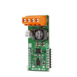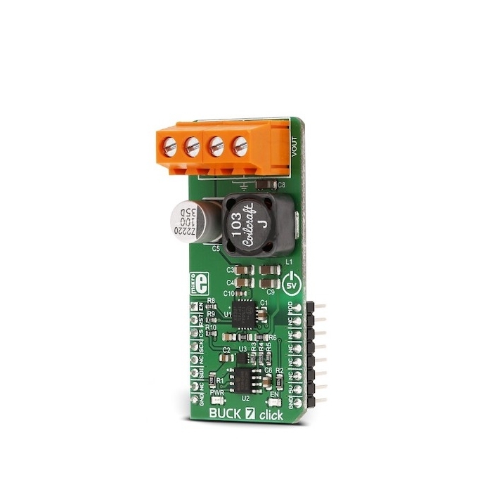
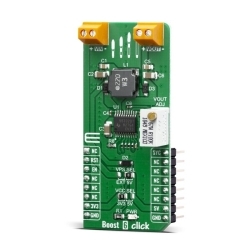
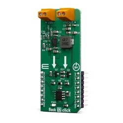
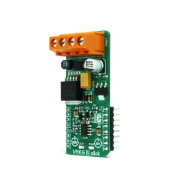
MIKROE Buck 7 Click
Buck 7 Click is equipped with the MAX17504, a high efficiency, synchronous step-down DC-DC converter with internal compensation, from Analog Devices.
Product Overview
Buck 7 Click is a high-efficiency buck (step-down) DC-DC converter, which can provide digitally adjusted step-down voltage on its output while delivering up to 3.5A of current. Buck 7 Click accepts a wide voltage range on its input - from 5V to 35V. The output voltage may be adjusted via the SPI interface, in the range from 3.3V to approximately 90% of the input voltage. This Click board™ utilizes the MAX17504, an integrated high efficiency, synchronous step-down DC-DC converter with internal compensation, from Analog Devices. In addition, to allow digital control of the output voltage, the MCP4921, a 12bit D/A converter with SPI Interface is used on the feedback loop.
This Click board™ is very useful for the development of applications that require programmed reduction of the input voltage, for various purposes. Features such as the low dissipation due to high efficiency, three different operating modes, overcurrent, undervoltage and thermal protection, output voltage monitoring pin, make this Click board™ very reliable power source for a range of applications, such as the distributed power supply regulation, wall transformer regulation, single board systems, general points of load, and similar applications.
Buck 7 Click is equipped with the MAX17504, a high efficiency, synchronous step-down DC-DC converter with internal compensation, from Analog Devices. This is an advanced integrated step-down converter, which requires a minimum number of external components, thanks to the internal feedback loop compensation. It utilizes a peak-current-mode control architecture, meaning that while the high side MOSFET is open and the current through the inductor ramps up, an overcurrent event will cause the MOSFET to close, preventing this current to become dangerously high. If there is a short circuit condition on the output, the device will reattempt to start after a timeout period, and if the condition is still present at the output, it will be turned off for another timeout period.
To allow adjustment of the output voltage via the SPI interface, the MCP4921, a 12bit D/A converter with SPI Interface made by Microchip, is used on the feedback loop. This DAC affects the current through the feedback loop forcing the PWM duty cycle of the internal generator, regulating the output voltage to a programmed value that way. As a result, by sending a digital value through the SPI interface to the MCP4921, it is possible to control the output voltage level in the range from 3.3V to 90% of the input voltage value.
While operating normally (PWM mode), the high and the low side MOSFETs are switched synchronously with the signal from the internal PWM generator, causing the current through the inductor to ramp up and down, regulating the output voltage that way. The lower pulse width (duty cycle) of the PWM signal, results in the lower voltage at the output.
Besides PWM mode, the device is also capable of operating in the PFM mode (Pulse Frequency Modulation). This mode allows even higher efficiency for light loads, as the low side MOSFET is completely unused. The high side MOSFET charges the inductor, letting the load drain it. During this period, the IC is in the hibernation state. This mode results in slightly more ripple at the output, with the added benefit of high efficiency for light loads. It is perfectly suited to power devices which are in the low power consumption mode (Sleep, Standby…)
The DCM mode is the compromise mode between the PWM and PFM modes. The low side MOSFET is still not used for light loads, but the PWM pulses are not skipped, and the IC constantly drives the high side MOSFET. This mode produces ripple at the output but it is slightly less efficient than the PFM mode for light loads.
Different modes are selected by the MODE pin. This pin is routed to the mikroBUS™ PWM pin (labeled as MOD), allowing the MCU to control the mode. When set to a HIGH level, the IC works in the DCM mode for light loads. When left floating, the PFM mode is selected. When it is set to the LOW logic level, the constant frequency PWM mode is set.
The #RES pin of the IC is routed to the mikroBUS™ RST pin. This pin signalizes problems with the output voltage. The pin is driven to a LOW logic level, when the output voltage drops under 92% of the nominal value, or during the thermal shutdown. It is an open drain output and it is otherwise pulled to a HIGH logic level (when not asserted)
To enable the buck converter IC, a HIGH logic level needs to be present at the EN pin of the IC, routed to the mikroBUS™ AN pin (labeled as EN). This allows the MCU to effectively control the Power ON function of the Click board™. When the IC is enabled, the LED indicator labeled as EN will indicate that the IC is activated, and the step-down conversion is in progress. Soft-start circuit prevents high inrush currents by introducing a ramp-up of the output voltage, from 0V up to the nominal value.


Features & Specs
- Interface: SPI
- Compatibility: mikroBUS™
- Dimensions: 57.15 x 25..4mm
- Input Voltage: 5V
- Output Voltage: Min. 3.3V, Max. 30V
- Input Voltage: Min. 5V, Max. 35V
- Output Current (continuous): Min. 0A, Max. 3.5A
Documentation
Customer Reviews