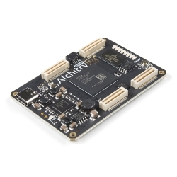
Alchitry Io Element Board
The Alchitry Io Element Board is the perfect way to get your feet wet with digital design.
Product Overview
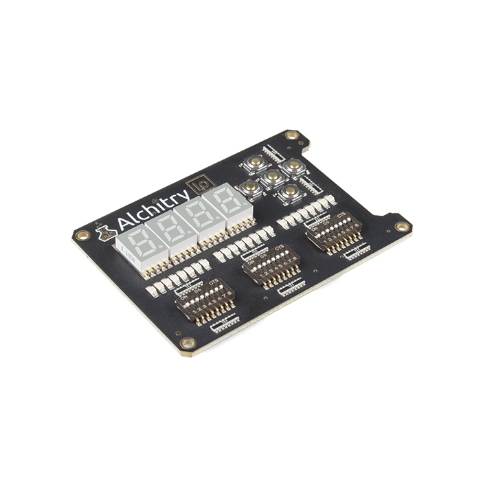
The Alchitry Io Element Board is the perfect way to get your feet wet with digital design. The Io features four 7-segment LEDs, five momentary push buttons, 24 basic LEDs, and 24 DIP switches that all lend themselves to fantastic beginner tutorials that will walk you through all the basics of FPGAs.
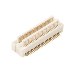
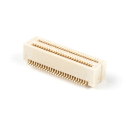
Alchitry Elements are expansion boards similar to shields for an Arduino or HATs for a Raspberry Pi but these are meant for your Au and Cu FPGA Development Boards. This Element is equipped with four connectors on the underside of the board that snap to an Au or Cu board. Be aware that the Io does not feature any connection points on the top of the board so you won't be able to stack any additional Elements on top of it.


Features & Specs
On this most recent revision (v2) external pull up capabilities for the R12 resistor were removed
- 4x 7-segment LED digits
- 5x momentary push buttons
- 24x LEDs
- 24x DIP switches
Customer Reviews

Stock and Customer Discounts
Available Discounts
- $25.60 | 10+ units
- $22.91 | 100+ units