
We make a lot of different designs in SparkX.
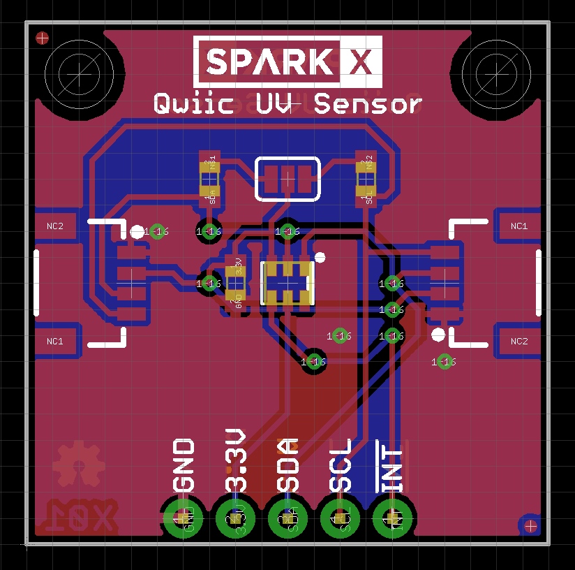
How do we get from a single design like the one above...

To a v-scored panel of UV Sensors that speeds up production? The panel is small enough that we can hand stencil it but large enough to pass the PCBWay minimum of 75x75mm for user-created v-scored panels.
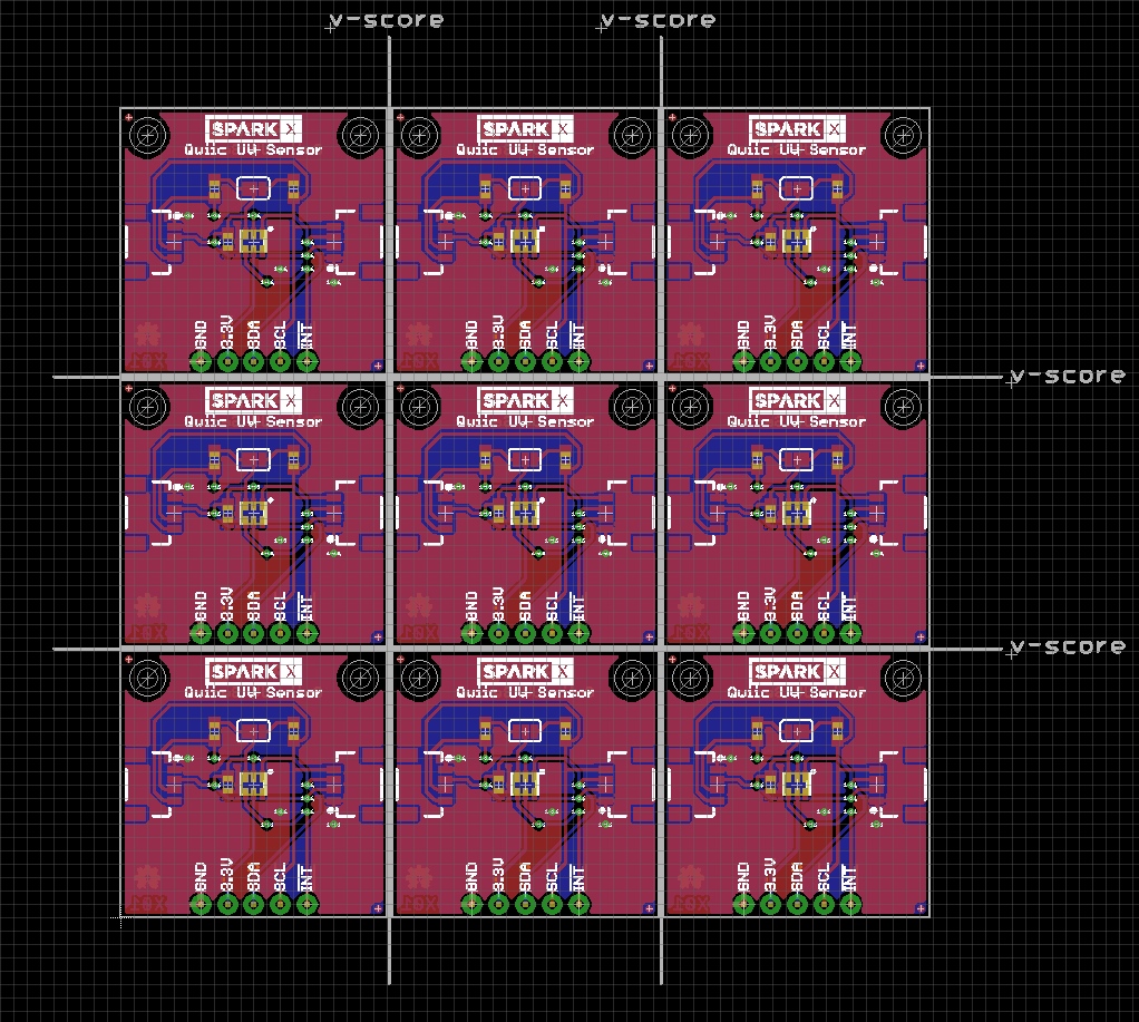
We used to generate these layouts like the one shown above by hand by doing the following:
- From the single board design file, turn on all the relevant layers
- Group select all the parts on the design
- Cut it
- Start a new BRD file
- Paste the design
- Move 0.02" to the right of the pasted design and paste again
- Repeat until you get to something larger than 75x75mm
- Add lines on the dimension layer to indicate where to vscore
- Add the words 'vscore'
- And NEVER forget to load the proper DRC file or else your vias will not be tented and polygon pours may become broken.
Yea, that last one is a doozy. EAGLE loads a default DRC file whenever you create a new BRD. The default rules are pretty far from what we run for production boards which always lead to vias being exposed and polygon pours being pull back from board edges which can lead to ground nets becoming broken. Oh my!
There's a better way! We've written a ULP called SparkX-Panelizer.ulp. You can get it and all our other helpful ULPs from our SparkFun Eagle Settings repo. However, to simply run a demo of this wiz-bang ULP:
- Download this zip and put the files in a directory you can easily navigate to
- Put the SparkFun-2-Layer-PCBWay-LIMIT.dru file in your Eagle\DRU directory
- Open the BRD file in EAGLE
- Click on the ULP button and run the SparkX-Panelizer.ulp
You should see a panel of UV sensor boards!
The settings such as gap between boards, min panel size, etc. are hard coded in the ULP but can be easily exposed through a GUI if needed.
We've got a new version! Please checkout our ULP repo for the latest SparkFun-Panlizer and SparkFun-CAMmer ULPs.
Let us know if you get benefit from this ULP and we'll try to share some of our other tricks. Thanks for reading!


I can't get either the old or new panelizer to work properly. The new version seems very buggy especially if units are in mm rather than inches. I probably have some thing not quite right because it's not handling the flooded signals. The last row is reproduced properly but everything else is messed up. It shouldn't try to do the math for the number of rows and columns, it should assume we're smart enough to do that ourselves. In the case of the first version, changing the 75 sizes didn't do anything. I could only get the result that I wanted by inserting the correct number into the program. Same with the new program.
Sorry you're having problems. We use it daily but it is very much tailored for our internal use. Feel free to post an issue on the repo. We add a new feature every few months.
I got the panelizer to work on my board, but the additional panels renamed all the components. If panel 1 has R1-R5, panel 2 has R6-R10, panel 3 R11-R15, etc. JP1, becomes JP2, JP3, etc. Is there a way around this ? I assume Eagle cant cope with two R1's on the same board. I suppose I could delete all the labels and use plain text to label the components, but that sounds a bit extreme. Any other ideas ? Thanks.
Hi, BigJon. I have the same exactly issue then you have. The devices names are renamed on the others PCBs, and thats a problem for production. Any one knows how to solve this?