PCB Bring-Up with SparkFun and inspectAR
InspectAR joins us today with a look into their easy PCB design tool.

This is a guest post written by inspectAR explaining the collaboration adding SparkFun's boards into inspectARs augmented reality PCB eCAD PCB tools, which enable electronics to work like never before.
The PCB Bring-Up Process
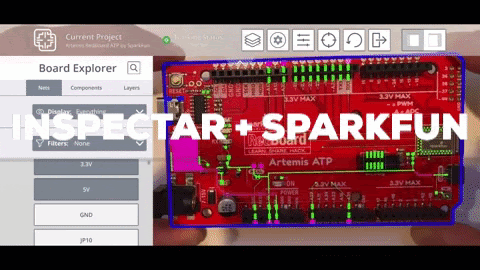
The SparkFun RedBoard Artemis ATP board with power rails highlighted under inspectAR
PCB design is a time-consuming and mentally exhausting process. There are so many competing manufacturing and design considerations to keep track of that it is no surprise most boards require at least one re-spin to create a functioning board. Especially if the original design wasn’t completed by the person now working with and debugging the board, as is often the case when working with various PCBs from SparkFun, Digi-Key and other major suppliers. The following article describes the board bring-up process once you have an assembled PCB in hand.
You will want the following tools to complete this process in a speedy and efficient manner:
- Your PCB
- Logic Analyzer (Saleae, Tektronix)
- Digital Multimeter (Fluke, Bryman)
- Oscilloscope (Rigol, TekTronix)
- Thermal Camera (Flir)
- inspectAR
Step 1: Physical Inspection Checklist
Impedance/Continuity testing
Once you receive your board, with the power still off, use a quality multimeter to check the continuity of each power rail at the input to each IC. All analog and digital power rails should show very low or even no resistance between the voltage regulator output and the IC power pin inputs.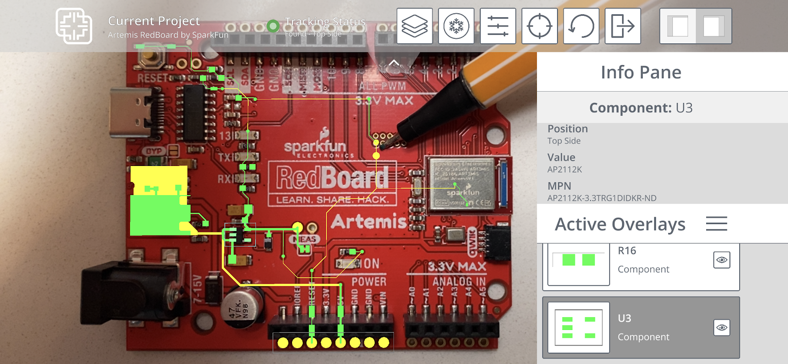
Sparkfun Redboard Artemis with power rails and components highlighted in inspectAR
Using inspectAR can speed up this process as you can easily highlight rails and ground contacts. Unless you have a resistor-divider in your system, the power rails should be isolated from one another, so typical resistance between power rails should be very high or have infinite resistance.
Optical Inspection
PCB components are very small these days. Look at your PCB underneath a microscope -- either optical or digital. You’re looking for a variety of potential issues that might lead you to either have to rework the board or return it to your fabrication/assembly house.Potential fabrication issues: Burrs /Mechanical Damage
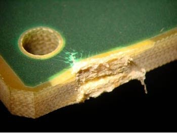
Can you see fiberglass fibers along the edges of your board or inside drilled holes? The presence of a rough or uneven edge may increase the potential for delamination of multi-layer boards.
Haloing
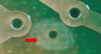
Haloing effect
A lightened area around a hole or via, typically induced by mechanical stress. Sometimes haloing will bridge two conductors that can lead to failures in a board later in time.
Copper Nicks/Scratches/Gouges
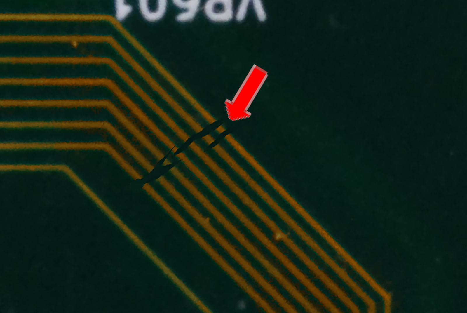
Scratch that results in open circuit
Did someone mishandle your board at some point before you received it? Are there visible scratches, nicks or gouges? If the trace is disconnected it may result in open circuits, among other issues, and you should reject the board and have a new one manufactured.
Delamination
Delamination
Sometimes boards get a bit too hot during the reflow process or are not laminated properly during fabrication. It’s not too common these days, but it still happens. Look for signs of delamination. Are there bubbles on the surface, or can you peel apart the edges with your fingernails? Does the color of the board appear to change to a lighter color over some specific areas of the board?
Crazing
Crazing
Can you clearly see the fiberglass pattern in a patch of the board? Do these areas go underneath connectors? Any of these signs can indicate that the board is starting to come apart. They are a clear indication that the board was delivered in an unsatisfactory state and should be rejected.
Conductor Issues
Copper bridging two traces
Do all the traces, pours and pads have well defined edges? Are there obvious copper bridges between adjacent traces on the surface of the board? Are there pin holes in the middle of a trace?
Board Bow/Twist
Severe Board Bowing
Is your board bowed, twisted or deformed? Usually this is caused by an asymmetric distribution of materials in the board stack up. If your board isn’t flat, there’s a good chance that there are components on the board that are not properly bonded to their pads. Like many of the other issues discussed, this is cause enough for a re-spin.
Missing /Misaligned Through Holes
Misaligned Holes
Missing through holes doesn’t happen too often, and usually can be traced back to an error made by the design engineer. If you are missing one, some or all your drills, you should trace the error back to the root cause.
Common Engineering Mistakes
Check your Gerber and drill files. Are the through holes present? Perhaps you made the mistake while you were adding the part to your library, or perhaps you neglected to include your drill file when submitting your job. Maybe a drill broke during the manufacturing process. A missing hole can mean a missing via, which can mean that you don’t have the net connectivity you think you do.
Manufacturing Mistakes
Modern manufacturers do not “forget” to drill holes in a printed circuit board. Most of the modern fabrication machines have cameras that monitor drill health and replace broken or worn drills. However, these machines do have limitations. Copper is a very tough material, and it can deflect high-aspect ratio drills rather easily. Manufacturers call this “wander.” The result is a hole that is not centered in a pad. Class 2 PCBs allow holes to break out as much as 90° from a pad, while Class 3 PCBs require no break-out and an annular ring of at least 2 mils. These are depicted in the following diagrams:
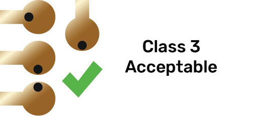
Acceptable Drill wander in Class 3 Boards

Acceptable Drill wander in Class 1 & 2 Boards
Lack of Adhesion
To see if the copper traces are really stuck to the board, press a piece of tape tightly against the board and pull it up. The copper should stay stuck to the board, and your tape should come up cleanly, with no piece of the board stuck to the tape.
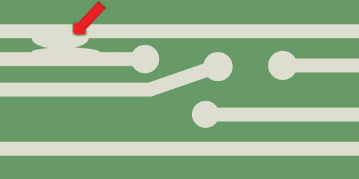
Tombstoning
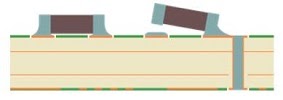
Tombstoning
Tombstoning is where one end of the component lifts from a pad of the PCB during the reflow soldering process, and affects mainly surface mount components such as resistors, capacitors and inductors.
Cold Solder Joints
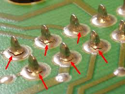
Cold Solder Joints
A 'cold joint' is one where the solder did not melt completely. It is often characterized by a rough or bumpy surface. Cold joints are unreliable. The solder bond will be poor and cracks may develop in the joint over time.
Solder Bridging
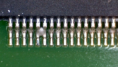
An example of Solder Bridging
Solder bridging occurs when two or more solder joints have melted together, forming an unintended connection between the two.
Mismatched Components
Components can be tiny, and often are only identified by their serial numbers. Ensure the correct components are used on your board. A simple mistake such as an AND chip in place of a XOR chip can completely change the function of the board.
Incorrect Orientation
Before soldering components, ensure they are correctly oriented, otherwise you could easily be connecting the GND to a power supply or worse, and possibly burn out the component.
Step 2: Power Supply Setup and Conformation
Polarity and Open/Short Checks
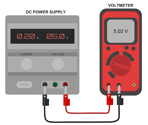
Most modern boards are powered by direct current. If you connect the power to the board incorrectly and neglect to place a protection diode at the power input on your PCB, you can destroy the components on your board in milliseconds. Take a moment to use a multimeter and ensure that the power supplied to your board is of the correct polarity and that there are no shorts to ground.
Check Power Supply Voltage
Engineers usually have more than one power source available to them, and it’s very easy to grab the wrong DC-barrel jack plug or set of wires and fry your board. Always get in the habit of using a multimeter to verify the potential difference of your plugs/wires. Ensure that you have the correct voltage out of your power supply – 12 V, 5.0 V and 3.3 V are all common supply voltages. You should check that you have selected the correct supply voltage to avoid damaging your power components, and check the inputs and outputs to each of your on-board power supplies and voltage regulators (Ido, busk, boost, etc.).
Set Current Limits
On the off chance that you have a short circuit, it’s always a good idea to set current supply limits on your power supply. Modern power supplies make this very easy to do. If you are using an unprotected power source, place a fuse holder in line with all positive and negative leads, and place appropriately rated fuses in the holder. If you have a floating ground, you should think about whether you should tie it to an earth grounding point through a properly rated resistor, connect it directly to earth ground, or allow it to continue floating. Ground leads are only fused in very specific circumstances.
Step 3: First Power On
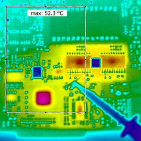
Temperature Check
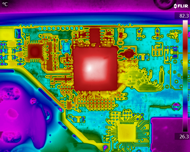
When PCBs fail, the result is usually either an open circuit, which does nothing, or a short circuit, which creates a great deal of heat. If the temperature is high enough, it can destroy a circuit board and the components that are on it. That’s why you should use a thermal camera or thermo couples to test the temperature of the board in a variety of areas.
Nothing beats a thermal camera for finding hot spots, but use whatever tools are available to you. If you detect a hot spot, you should turn off the power supply immediately and investigate. You never want to “release the magic smoke” from a component. Once it is hot enough to vaporize parts of itself, the component is ruined.
Check Power Rails
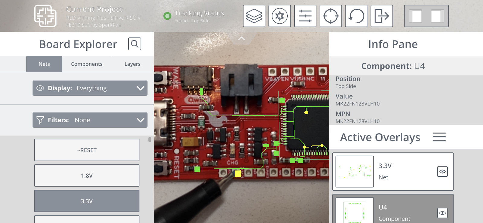
Probing and measuring voltage rails being highlighted using inspectAR. In this example, we are using a SparkFun RED-V Thing Plus
Once the power is on, connect the black lead from your multimeter to ground and use the red lead to probe the power rails. Ensure that the rails have the correct voltage.
The inspectAR application can easily highlight nets and pads to show the user where to place their probes. In addition, with components the application clearly highlights each pad and the net connected.
Quick-Start guide to setting up inspectAR:
- Create a free account and download inspectAR online or from the mobile app stores. The free application works on mobile and allows users to use inspectAR with pre-loaded boards from SparkFun and other distributors and sponsors. The professional version allows users to use inspectAR with their own, custom PCBs on mobile, tablet, PC and Mac.
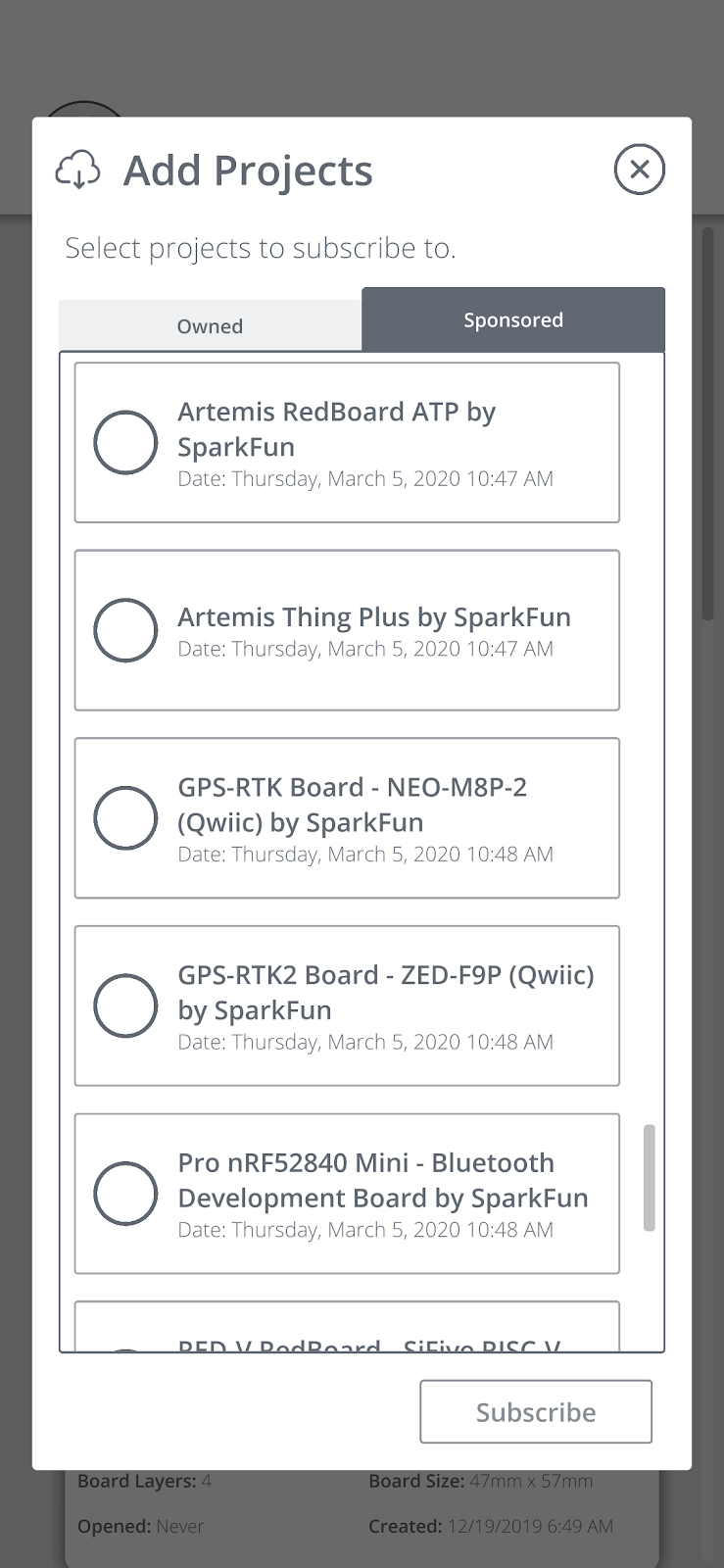
- Log into the native application and find some pre-loaded projects to subscribe to. There are plenty of great boards from SparkFun available, with more coming regularly.
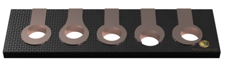
SparkFun boards pre-loaded in inspectAR, available for all users (Free + Pro)
- Once you have subscribed to a board or two, your project dashboard will look like this:
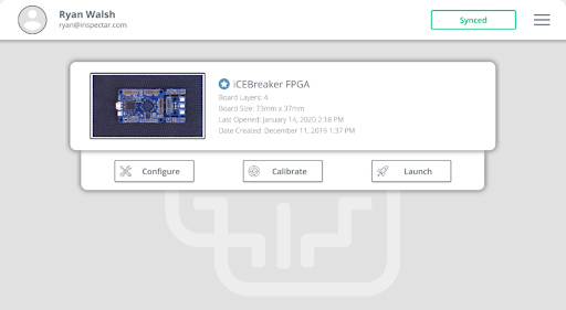
Project Dashboard showing an iCEBreaker FPGA Development Board, available on SparkFun
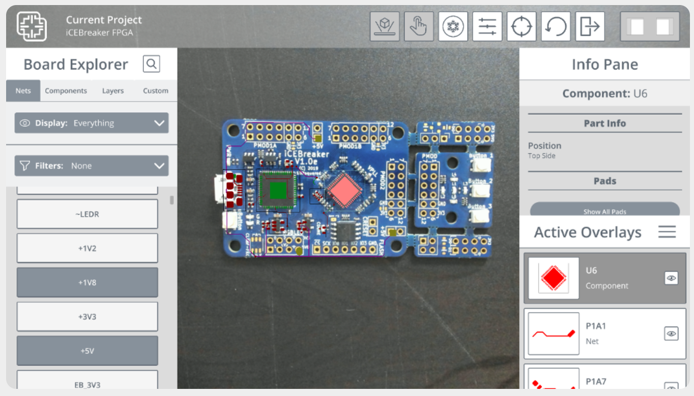
- Most pre-loaded boards come with a default calibration. If you find any of the augmented reality overlays to be jumpy or offset at all, you may want to re-calibrate your board under your operating lighting and background environments.
- Launch the AR scene, and get started!
- For more information on getting started, along with details on every part of the application, head to the inspectAR support site. You can also get information on using inspectAR with your custom PCBs there.
Oscillator Checks
Modern MEMS-based oscillators are relatively foolproof, but crystal oscillators can still give engineers headaches. Use a non-contact or near-field probe on an oscilloscope to detect the operating frequency of your clock signals. Ensure that your device is running at the desired frequency. If, for example, your program assumes a 20 kHz clock signal, and you’ve accidentally called out a 25 kHz clock on your BOM, your device may not function and the timing of your asynchronous serial interfaces will be wrong, which means you will not be able to debug your board over UART.
NOTE: Ensure you have added a bias resistor in parallel and refer to the crystal datasheet.
JTAG Pinout Confirmation
Unfortunately, there are several JTAG patterns for PCBs in a variety of pitches. You need to ensure that your JTAG programming cable will mate properly with the PCBs JTAG pattern. If not, you will need to purchase or make an adapter that allows your programmer to communicate with your PCB.
Tag-Connect is a popular “plug-of-nails” that allows header-less connections -- if you use one of these devices, it is very easy to move from one board to another without worrying about reversing the connection.
Pre-flash Thermal Profile
Thermal Profile
You might consider leaving your board powered on for several minutes before you first load code on it. This gives you an opportunity to characterize the thermal properties of the board with a thermal camera. Later, when you add the firmware, you can run the test again. The difference in the thermal profile running your code and the temperature profile without code gives you an indication of the power consumption of your code.
Step 4: First Programming
Get to Blinky!
Most boards have some sort of controllable LED. An easy first step to ensure you can program the main microcontroller and actually interact with the hardware is to get the LED to blink in some capacity. Here’s an example of “getting to blinky” with an Arduino. Additionally, this is a great time to run through most of the available GPIO pins and see if you are able to toggle them on or off with software. Put a statement in your code to toggle a GPIO pin or read the state of a switch. The idea is to get positive confirmation that you are controlling the target integrated circuit.
Prepare to Debug
If your IC already has firmware on it, you should take a moment to read and save it to your computer. Debug, debug, debug! Put statements all throughout your code -- at counters, at loops, at the start and end of each function. The idea is to make the debug statements so abundant that you can trace a bug down to a particular function, and perhaps a certain line of your code.
Then compile your code and upload it to your target IC.
Open Debug Port
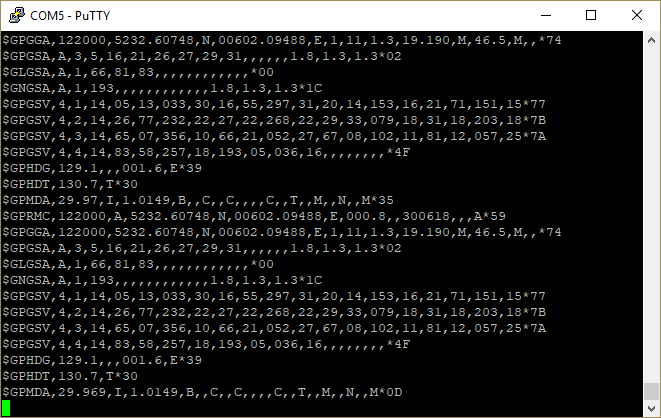
PuTTY output
Almost all firmware programmers can program and debug, so open a debug port and hope that you see some form of debug information streaming in. Alternatively, if you have enabled a separate UART port, connect an external USB-to-UART converter (such as Silicon Labs CP2102n), configure the transmission speed and view it with a program such as PuTTY.
Post-Flash Thermal Profile
Once you get your firmware up and running, let it run continuously for a while and point a thermal camera at it again. The difference in temperature profile between running with code and running without code can give you an idea of how much power your device consumes.
What to do when things go wrong
Stay Calm
Start with the problem area or component. Go through component by component, pin by pin. Backtrack. Using inspectAR (or your EDA tools), you can highlight components and backtrack from problem to source by incrementally adding overlays for nets connected to pads, probing, then continuing down the line. Understand all assumptions and calculations made in the design, confirm that each component is assembled where it should be, and that the value and package for each component is what you are expecting.
Your DMM, Oscilloscope, Logic Analyzer, and inspectAR are your best friends in this scenario. You can even get on a video call and walk through the board with your team, no matter where they are! Highlighting traces and components in real-time with inspectAR makes this much easier.


