And we’re back! Today we’re going to wrap up our PCB design series with taking a look at the more creative, customizable aspects of design. This involves changing up our board shape, importing images on to the silk screen, and learning how to add mounting holes for things like keyrings or stand-offs. This is my favorite type of board design to do, so let’s get this ball rolling!
In case you missed it: be sure to check out the rest of the series to learn how to go from a schematic diagram to a THT or SMT board!
Components
Alright, we’re going to keep our circuit simple and focus on the board, so here’s a list of the parts I used with mine if you’d like to reference those:
- Battery: C964831
- Button: C10852
- Resistor: C101329
- LED: C2286
Since we’ve already covered creating a schematic diagram and placing and connecting components on the board, we’ll skip going over that step here. If you missed that info, or need a refresher, be sure to check out the previous EasyEDA blog posts; for my design I went the SMT route but you can, of course, use THT if you’d prefer!
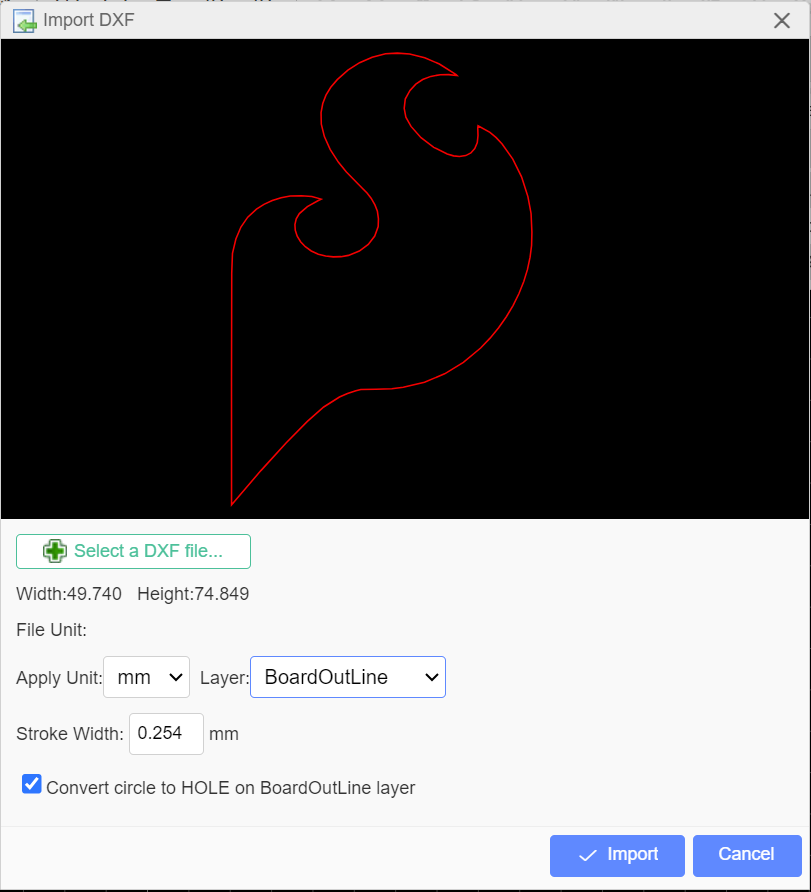
Import a .DXF for the Board Outline
The first thing you’ll need to do is find some shape that you want your board to be: the simpler the image, the easier it will be to get an outline from it. Then, take that image into an editing software of your choice; I use Inkscape since it’s free to download and we don’t need lots of bells and whistles for this, but anything that allows you to generate a .DXF of your outline will do!
Once that’s ready to go, generate your PCB and delete the default board outline. Then, go up to File → Import → DXF… and select your file. A preview of the file will popup, with a size description beneath the ‘Select a DXF File…’ button; one thing to keep in mind is that JLCPCB has an additional charge for boards exceeding 100x100mm and the size will be imported from your DXF file. I wanted mine to be keychain sized, so I made sure to note that when creating the DXF of the outline I wanted (which looks vaguely familiar, don’t it?). With the dimensions good to go, all that’s left is to ensure that our layer is set to ‘BoardOutline’ in the dropdown menu.
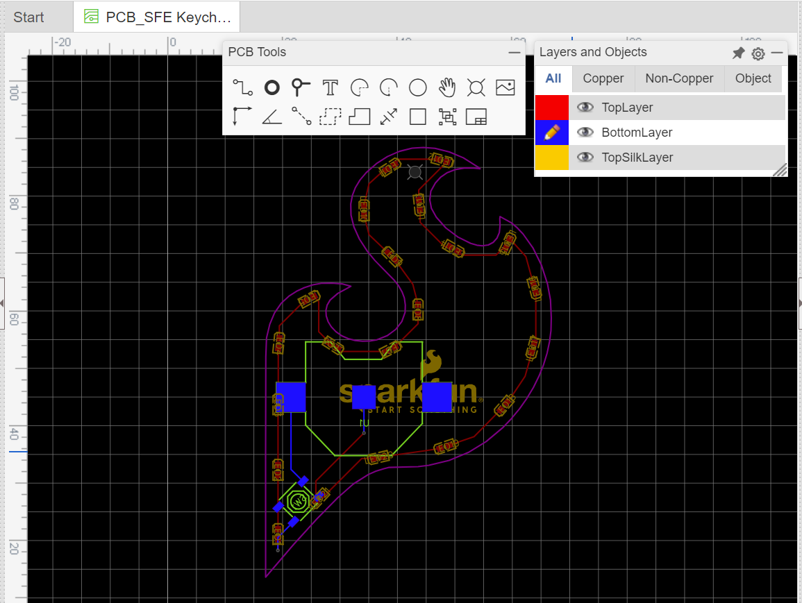
Orienting Parts Along a Curve
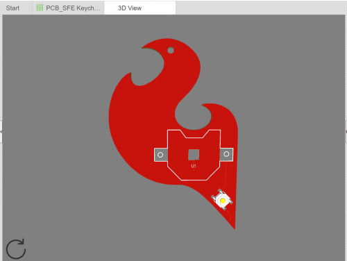
Now that the outline is in, we can place and connect our components how we’d like! Since my board has these fun curves, I wanted to replicate that shape with my LEDs:
The easiest way to do this is to select the part and drag the green dot around until it’s laying how you want it. You can also select the part and type degree values incrementally in the box labeled ‘Rotation’ on the right side of the designer.
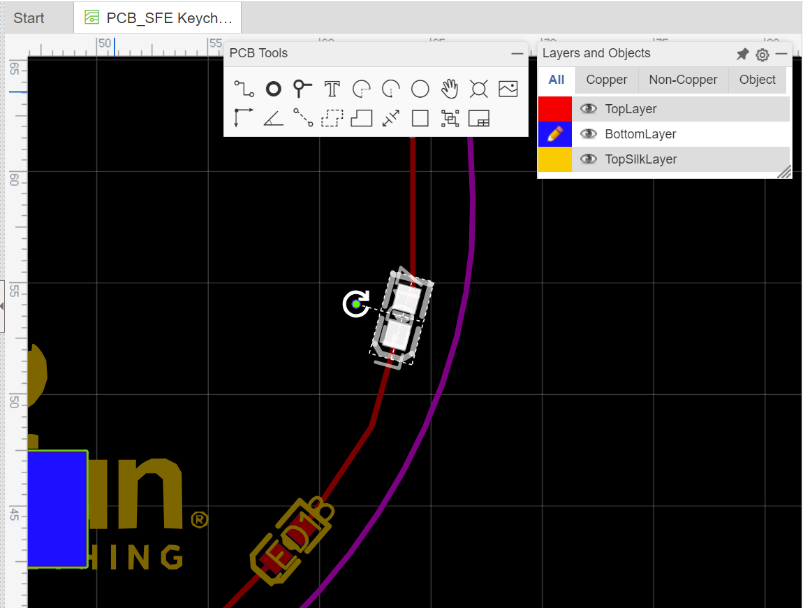
One thing to be aware of when orienting parts outside of 90 degree increments is how you plan to place them when building the board. The easiest option is to order them fully built from JLCPCB since they’ve got all the fancy toys for manufacturing boards. Hand-placing, while time consuming, is a good way to be able to control the orientation yourself, but can get a little confusing and is easy to bump parts out of place.
The last option is to use a pick and place if you have one at your disposal. I have worked with the CHMT36VA from Charm High with curved part placements in the past, and it did great with them; I was building a lot of boards and did notice a bit of drift over time, but it was a quick recalibrating and we were back on track! If you’re interested in learning more about that machine, check it out here:
Creating a Custom Silk
Next we’re gonna look at incorporating a custom silkscreen on your board; this process is very similar to the board outline, where you’ll navigate to File → Import → Image… and select your file (you can also just select the image icon from the PCB tools bar and that will open up the same prompt window). Keep in mind, when selecting what you want to add, that the silkscreen is a single color; playing with positive and negative space allows for a lot of dynamic imagery, but can’t quite do it all.
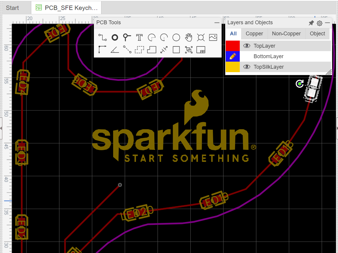
One last note with this: the images usually place on the TopLayer by default, so be sure to select it and change the dropdown on the right hand side to ‘TopSilkLayer’, otherwise it’ll build as a copper area and be covered by the solder mask. Which, you’d still be able to see on the final board, but will interfere with your traces if they happen to cross paths.
Adding a Mounting Hole
Last up, we’re going to check out adding a mounting hole to the board: these are great for standoffs, screws, keyrings, pretty much anything that attaches your board to something else. This is a really simple step, with a few things to note; select the circle with the X behind it from the PCB Tools bar and place it wherever you’d like. By default, the diameter is 2.032mm and, depending on what you’re looking to thread through it, you can change this (with the part selected) on the right hand side. For keyrings, I find that bumping it up to 2.500mm is sort of that Goldilocks zone. If you’re putting a screw or standoff through it, grab some calipers and measure your hardware to get a good fit.
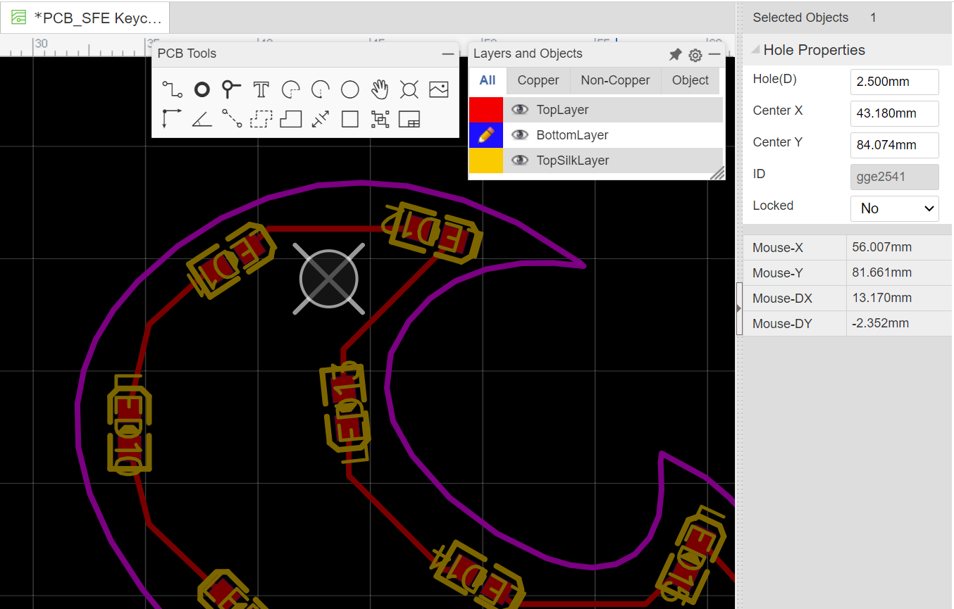
Now, you’ll want to consider what material is going through the board as well; although I didn’t with this design, if I had built out a copper area as a VCC or GND plane, running a piece of metal through a hole in the board could end up shorting it out. If you’re using copper areas it’s always a good idea to isolate around holes in the board just in case. I had a keychain PCB I made a while back that ended up shorting from the wear of it moving around the metal keyring over time; it was still fun to look at but it didn’t light up anymore, which is just simply not as cool.
That’s all, folks!
Thank you all for joining me for this mini-series, and I hope you are encouraged to check out the wide world of PCB design. If you do end up dabbling in it, or going all out, please be sure to share your projects with us!
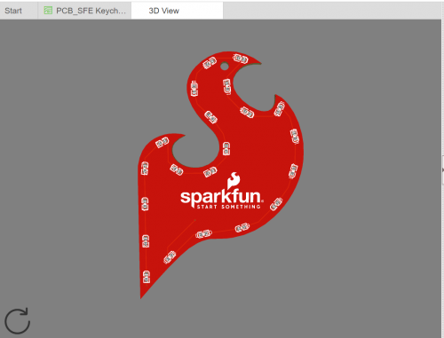
For those interested, here’s the final look at the 3D view of the board we were working with:
Designing your own PCB? Tell us how it went in the comments below, or show us on Twitter, Instagram, Facebook or LinkedIn.


