Enginursday: KiCad and Open-Source Design
The process of using open-source designs to get to a final product, featuring KiCad, PJRC, and Advanced Circuits.

Buckle up kids, it's Enginursday! This week I bring you the process of using open-source designs to get to a final product, featuring KiCad, PJRC and Advanced Circuits.
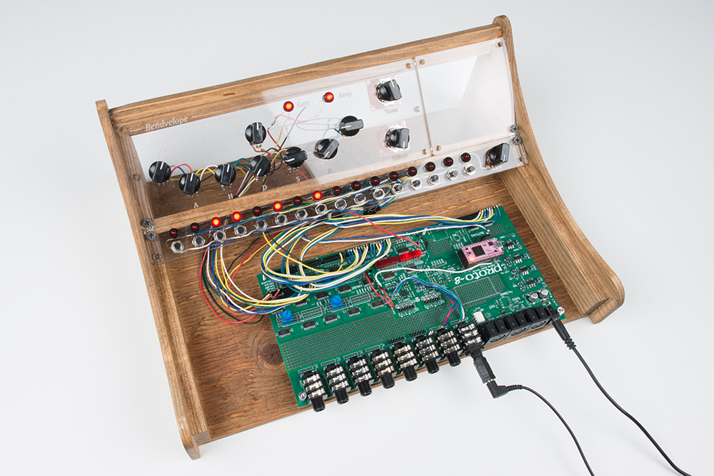
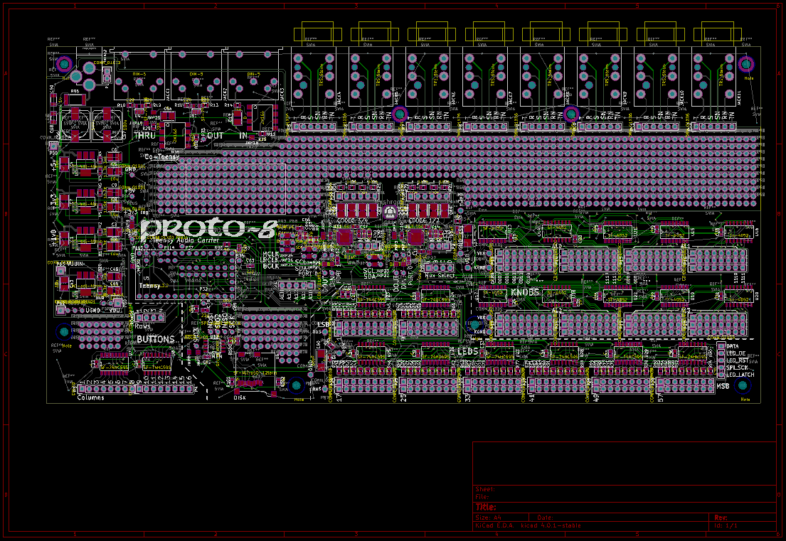
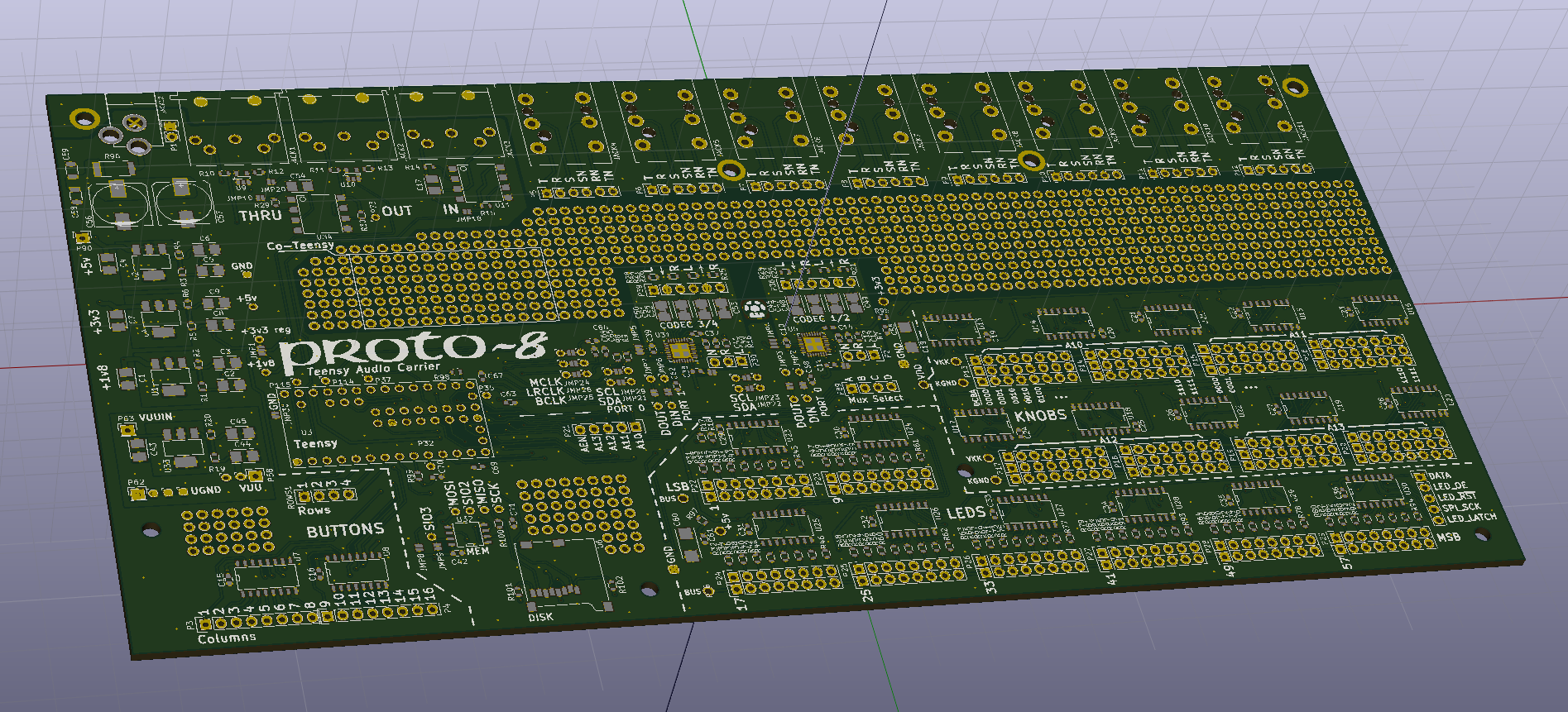
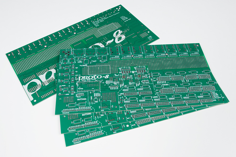
A test and programming fixture that supports the Proto-8 board and allows me to test new PCBs, as well as program for different types of panel sections. This is the completed final goal of this KiCad experiment.
As a hardware engineer, a program is a thing that lives in a black box and it's up to me to get it out. Looking at a standard 328p type development board, this means adding knobs, buttons, displays, and periphery that control or can be controlled by the program. So, solder on some wires and breakout boards, zip tie the whole thing together and you've got yourself a bonafide prototype.
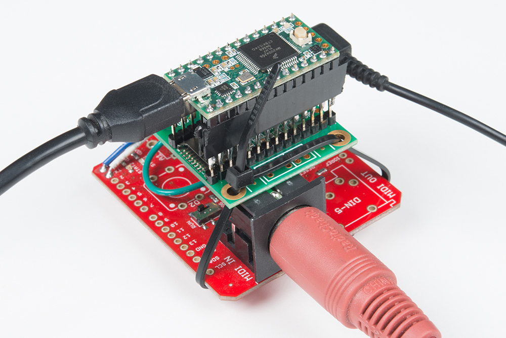
This is what the original prototype looked like. It uses two of PJRC's designs that are *generally connected as intended, though I could have made use of the Teensy Arduino Shield adapter board.*
But my prototype doesn't have any knobs on it! As a prototype, it uses the midi bus to get knob data from a midi controller, allowing me to test my code. It's a convoluted process that involves double checking IN/OUT cables, using counter-intuitive midi controller programming/bank selection, and a nasty spreadsheet that maps controller numbers to parameters so I can keep them all straight.
What I'd like to do is just wire knobs to it. Unfortunately, micro-controllers only have so many pins, and I want more. Lots more. Hundreds. And I don't want to solder all these goofy wires and muxes together. It's time for a prototype PCB.
Create the Spec
Specifying was an interesting lesson in college. The only time it was really talked about was during senior design, 4th year. The students prefer a hard-and-fast set of rules that they can blindly follow, but the process of figuring out a product's final form can be highly organic.
For this project, I discussed thoughts with fellow engineers. Scribbled on white boards. Wrote lists, then threw them away. I asked, "How big is it? How many features are there, and what are they? What voltages will it operate from?" Eventually I came to a list of things that would always be present, and I knew I had a place to start.
Find Some Reference Designs
At this point I'm about 80% sure what the product will be, but focusing in will have diminishing returns so it's time to get what I know down on paper.
This is where the open source comes in. I know I want it to have MIDI ports, teensy audio, and some button matrixing, and the thing will need some power. I collect the following references:
Armed with these, I can approach the design.
Get the Components Ready
This is a little bit of a leap. I haven't done any design yet, but from experience I know the next "productive" step is to enter the schematic into the EDA (electronic design automation) tool, flip to layout and start drawing. BAM! There it is. In order to use a component in a schematic, I need to have a symbol, which I may need to generate myself. I don't want to be making a new symbol every time I need one, I want to start my schematic and do it all. The solution: Get all the components ready first. For your own sanity.

Here's what sat on my desk during the early phases. It's hard to trust component conversion tools, so I like to have a reference for the odd stuff.
There are a few things to do to make new parts. Get the datasheet for each part not currently in the library. If possible, I like to have the physical component on hand as well. Often I notice something not drawn in the mechanical section. The datasheet also serves as a guide on how to make the symbol. When in doubt, draw it like the manufacturer drew it. It's convenient to also make the footprint at this time, and having the component in my hand allows me to move it around with other components and think about what a reasonable distance between components would be, and to double check mirroring of the layout. If I can see the part, I know if I'm looking from the top or bottom.
KiCad's component system is a little different from the Eagle system I come from. In KiCad, the component symbols and footprints are kept in separate files. Between the schematic entry and layout phases, footprints are associated to components in the schematics (using the CvPcb tool).
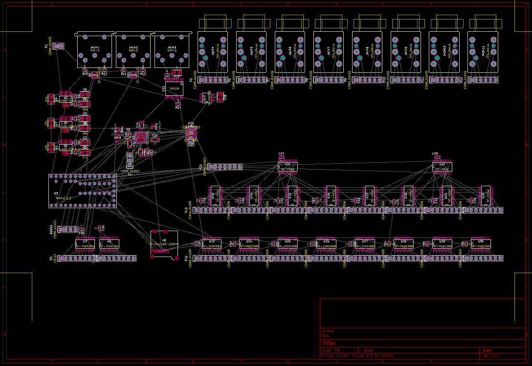
Enter the Schematic Design
With references and components in hand I can start the schematic. I go back and forth between researching stuff and entering diagrams. I've found that even if I think I've covered 100 percent of the design, I realize what I forgot as soon as I try to enter the schematic. Often the realization comes as a, “Wait a minute, what's this pin for?” thought, or, “Wow, I drew this symbol way out of scale!”
The general idea is to convert all reference designs into schematics for the tool. First, enter the core of the reference design -- that is, things that connect only to other things in the original design. Then, connect the cores together. For me, I entered the following cores:
- The midi shield core
- The Teensy schematic diagram
- The power supply (LDO) stuff
- The codec as in the Teensy Audio board
Using the reference designs allows me to trace connections through the original product's ports in order to get them wired up correctly. I could stare at tables in datasheets until I'm blue in the face, but I'd still have a chance of swapping TX and RX. With the reference designs, I get to see what worked for someone else.
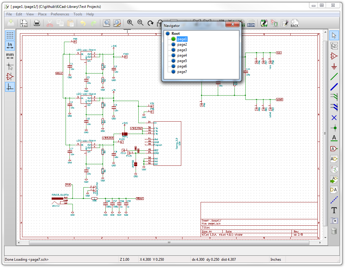
Eeschema schematic capture tool with page navigator shown.
When all the reference designs are in there, kind of as-is, it's time to connect the various designs as stacking the shields would have done. Remember the zip-tied stack of proto earlier? I need to make those connections. Again, I start with what I know, and create lists of the things I hadn't thought about while doing what I know.
An example that came up while working with the LDO (Low-dropout regulator) sources was the option for using the Teensy's output regulator to source the 3.3v rail. I was planning on using an LDO for this rail and hadn't thought about the Teensy's regulator until I saw the pin in the schematic. This lead me to use a three-position jumper to allow sourcing from either. This came in handy when my 10-year-old prototyping resistor on the LDO's feedback started to drift, and I was able to swap over to the Teensy. It's little decisions like this that can lead to a good product, but can also lead to scope creep and over-engineering.
The best part about open source is that a design can be modified if it doesn't suit a need. I wanted a third MIDI port to use as a thru, but maybe for some other purpose. I combined the IN and OUT parts of the shield design onto a single jack so that either function could be selected.

Condensing the MIDI shield's design into a single multifunction port
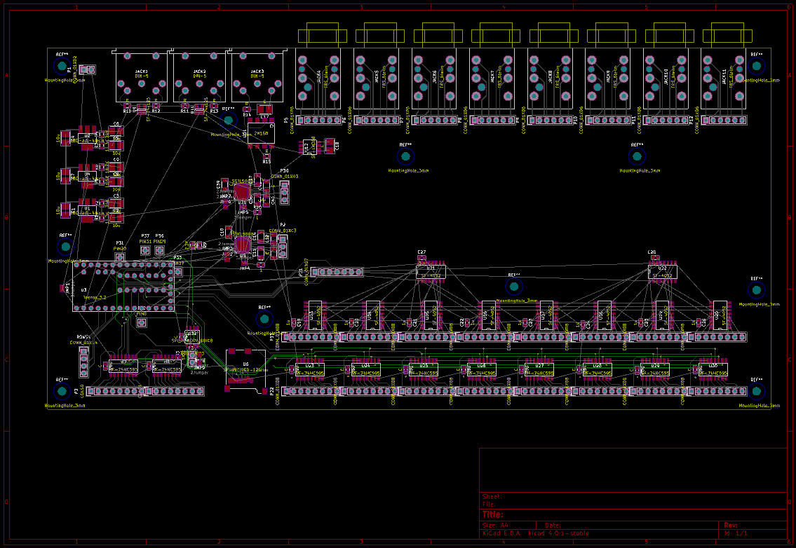
Start the Layout
Having received enough abuse from the schematic entry tool, I needed to see what it would look like on the board. Eagle is nice because it handles synchronization between schematic and layout automatically. KiCad does not, which can be good and bad. The bad side is that I have to figure out how to do it myself, but the good side is I have more control over the libraries and associations. Do you want to associate that 1x8 0.1" header to an 8-pin IC symbol? Sure! Go right ahead!
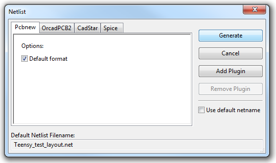
Where Eagle uses a single button to switch to schematic, KiCad makes you do a dance. First, I annotate the schematics. This goes through and applies names to all my unassigned components. It works page by page in horizontal or vertical scanning fasion, applying names like JACK9 and U14, etc. The next step is to associate footprints to the symbols in the schematic. Having done that, a netlist is generated and saved. This netlist is what the layout editor uses to decide what exists and how it is connected.
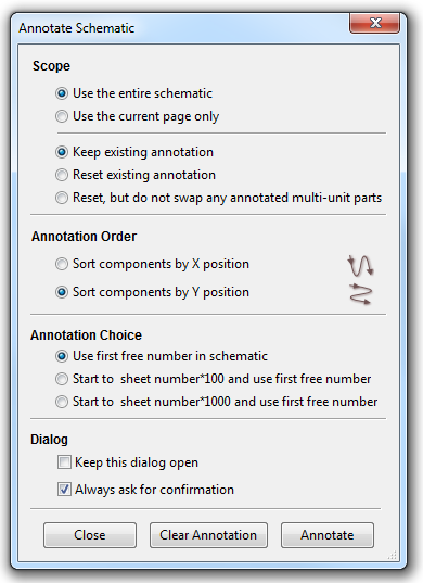 Use "Annotate Schematic" to apply reference designators |
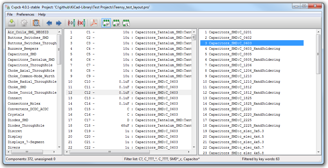 Pick a footprint for each component using Cvpcb Pick a footprint for each component using Cvpcb |
 Generate a Netlist for the layout editor (Pcbnew) to use Generate a Netlist for the layout editor (Pcbnew) to use |
All the work up to this point was really to answer one question: “Do the layout ability and interactive trace dragging features of KiCad work, and are they useful?” I know, that's a lot of legwork just to play around with an open-source interactive router... what am I saying? I've been wanting for this for years! Let's get in it.
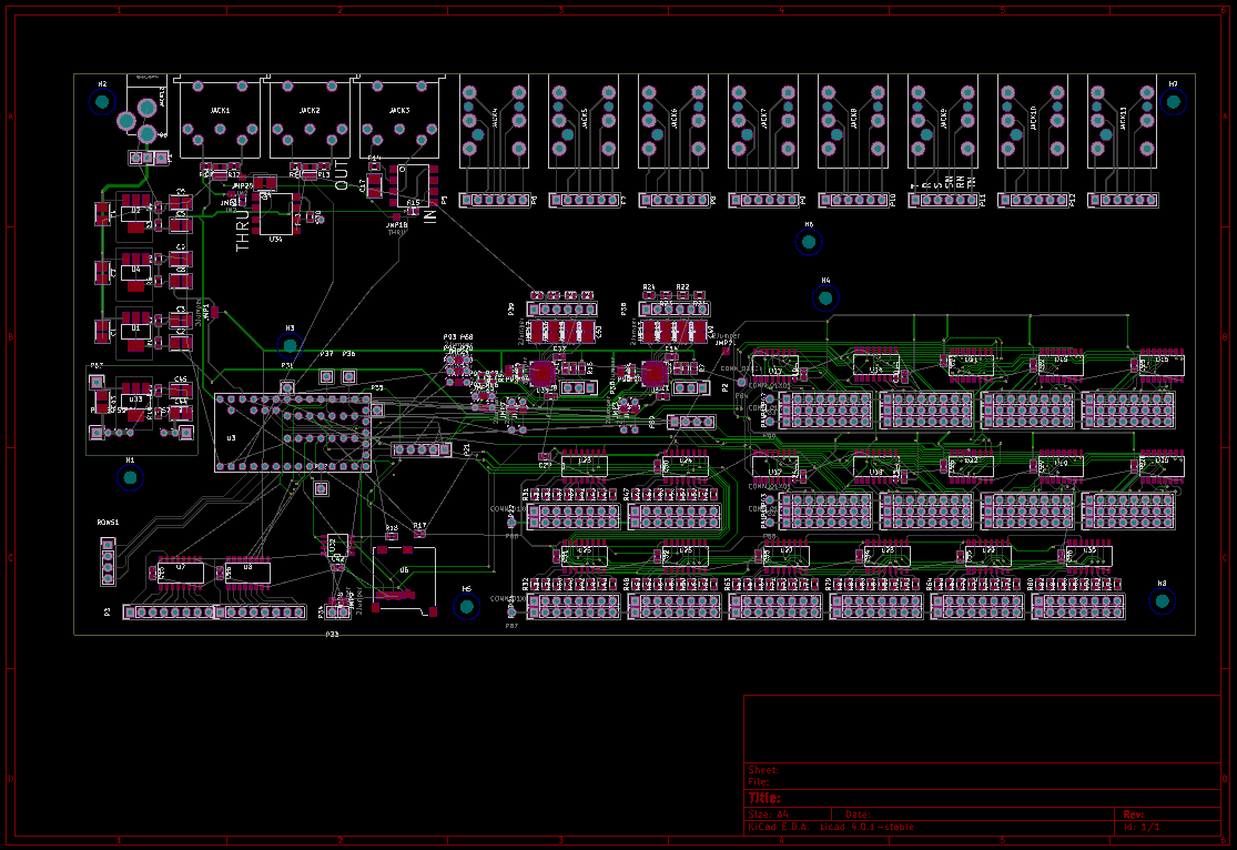
Iterate!
It wouldn't be Enginursday without a diagram that oversimplifies the engineering process! This time it's to show that the layout didn't just happen. Something was tried, and the validity of that idea was considered, and a new thing was tried.
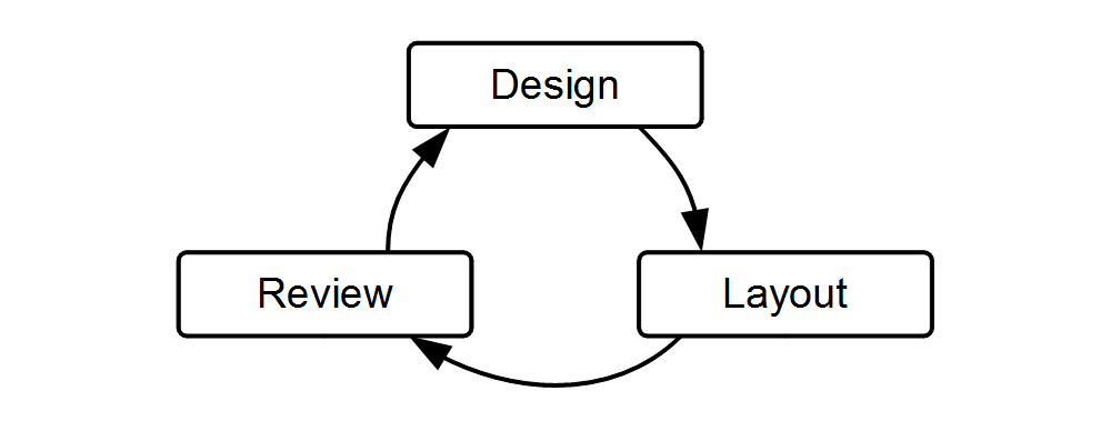
The iterative layout process
For this design, I started with a smaller board and experimented with various orientation sections before coming to the final solution. Sometimes I tried doing a little routing here and there to see if I was on the right track. In the following pictures, I show snapshots of this progress. I think it's interesting that the difference between the early designs is huge, while later in the process the changes are more of a refinement, and not much major movement occurs.
 |
 |
 |
 |
 |
 |
 |
 |
KiCad and Layout
To me, the thing that makes KiCad stand out as an EDA tool is the ability to do interactive routing. Having worked in a button-up engineering firm, I always saw the PCB department dragging traces around. It looked a lot better than the 'ol rip-up and re-route method I was used to.
A quick demonstration of what interactive routing can do
To get KiCad to do this, it needs to know something about the signals and how close together they can be. The clearance of traces (and default widths) are set within the Design Rules Editor, a function of Pcbnew. I found that it was easy to set up various rules, and that they are mappable to any of my signals. I ended up with four signal classes (Jack Interface, JackLine, Power, and Signal, plus default) and was able to get all the spacings I desired.
Calculating and displaying moving traces is also quite a task. KiCad handles this by using OpenGL, which is turned on in the layout editor. Some tasks work in OpenGL mode, like interactive routing, while others didn't work so well. I found the OpenGL mode had troubles setting an origin right on grid. It wanted to snap to other places that didn't make any sense. But, the native display mode had great snap to grid. The open-source solution is to switch between the modes with the function keys.
 Viewing the layout using native graphics (F9 view) |
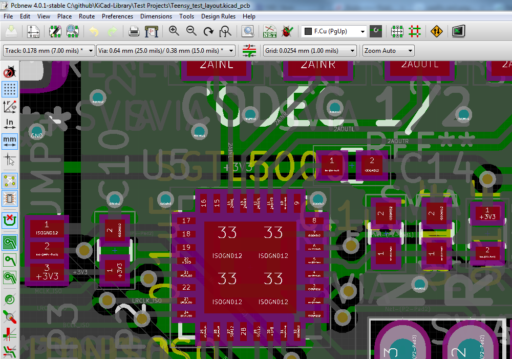 Viewing the layout using OpenGL graphics (F11 view) Viewing the layout using OpenGL graphics (F11 view) |
I found a lot of features of KiCad seem to work best with hotkeys over navigating menus. Once I learned them, their usefulness was apparent, like B and CTRL-B to fill and un-fill polygons, and the mouse-centering feature. I view a lot of open-source software as something unrefined where I need to learn how the programmer liked to use it in order to get the most from it. Fighting with an open-source tool because it doesn't work how I'd like usually ends in frustration.
Finish and Prepare for Fabrication
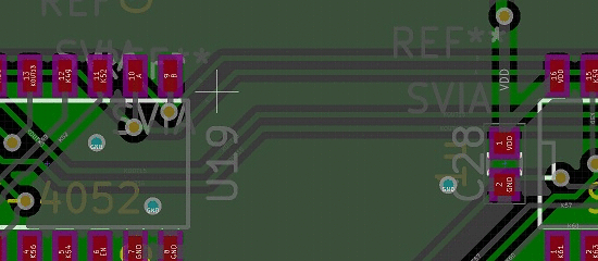
When I'm finally happy with where the parts will be, it's time to start tweaking. I chose to use reference designators on the silk, which means they need to all be the same size and placed in useful locations.
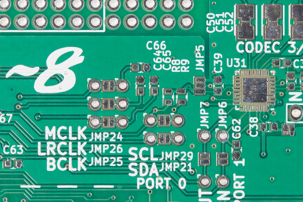
Here I've shown one technique for arranging designators. I didn't have the room to just put them side by side, so I arranged them as the components are arranged and put them in a group. Notice that the orientation and offset of C66-65, and R8-9, are a match to the 0603 pads nearby.
Once the designators are done, I took a moment to show some pride and dress it up in silk. The KiCad bmp-to-shape tool is as buggy as everyone else's, but I had success. I found the best method was to get something meaningful to come out of the tool, measure how big it is, how big I want it to be, then re-process with a different scaling factor.
Another oddity I found was that the tool would only produce silk layers. It's open source though, it's open for me to look at! I found that the footprints are saved as text, and noticed that I could change the layer tag to move the layer.
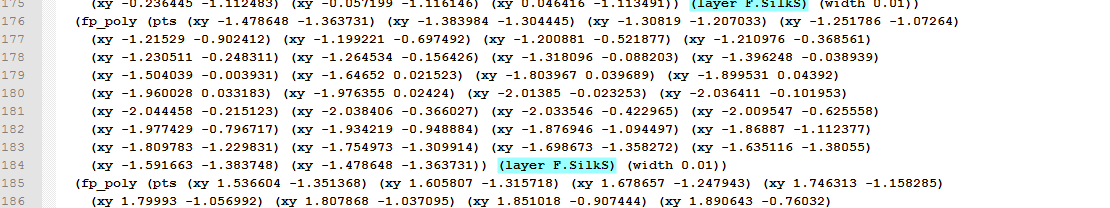
Each polygon has a layer attribute which can be manually modified
Another tool I found useful was the board render feature.
The KiCad render function gave me a great sense of what the board's aesthetic would be. The render also provides for models, but I didn't make my components with them so I turned the feature off.
With the board looking good, it was time to check if the board meets the PCB manufacturer's rules. I ordered boards through Advanced Circuits $33 each proto service, which lists the minimums clearly on the landing page. This service comes without an electrical test, so it's possible I made shapes that can't be fab'd and no one noticed. The interactive router used design rules so it forced clearance, but running the DRC popped up a bunch of hidden copper and unconnected traces that looked connected. It's good to use the rules and run the DRC.
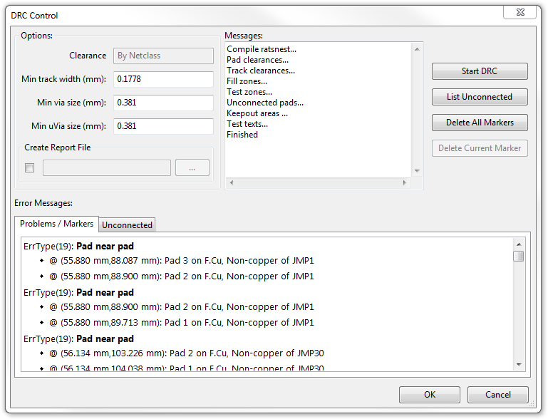
The DRC report. The remaining errors are solder jumper pads that are too close together; this is expected.
The last step was to produce gerbers for the manufacturer, which KiCad handled like a champ. It also has a nice feature for viewing gerbers, which turned out to be more beneficial than I imagined. Many PCB services offer a gerber viewer, and the demos look great, but I couldn't get it to function on my home computer. KiCad's viewer was the last time I saw the design before getting a package of PCBs in the mail.
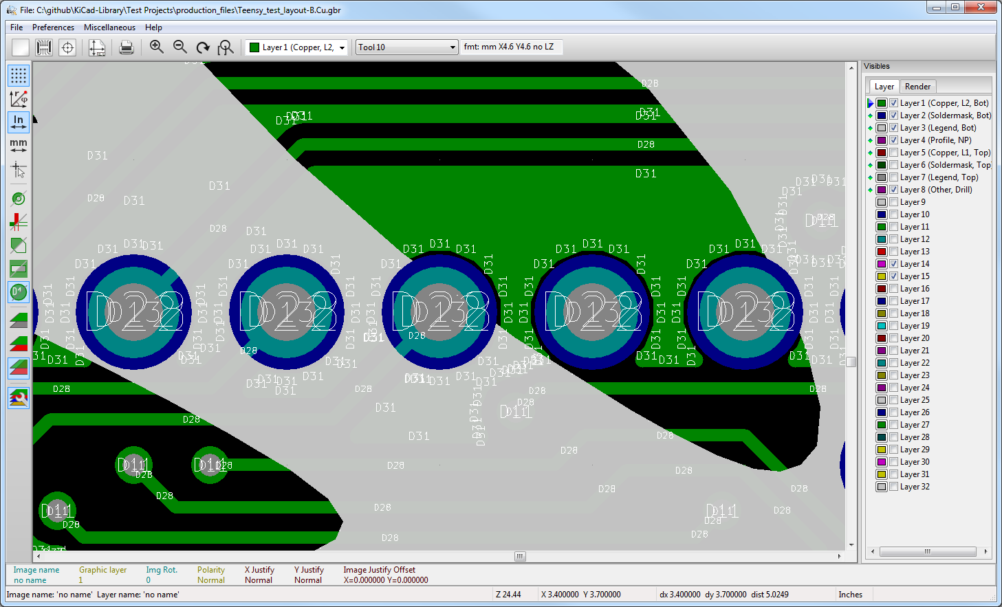
The GerbView program. Here, I'm checking to see that the silk layer was cut out around the PTH annular rings. I didn't notice before, but I could have pulled in the mask stop to ease alignment of the PCB layers and prevent the copper edge from showing.
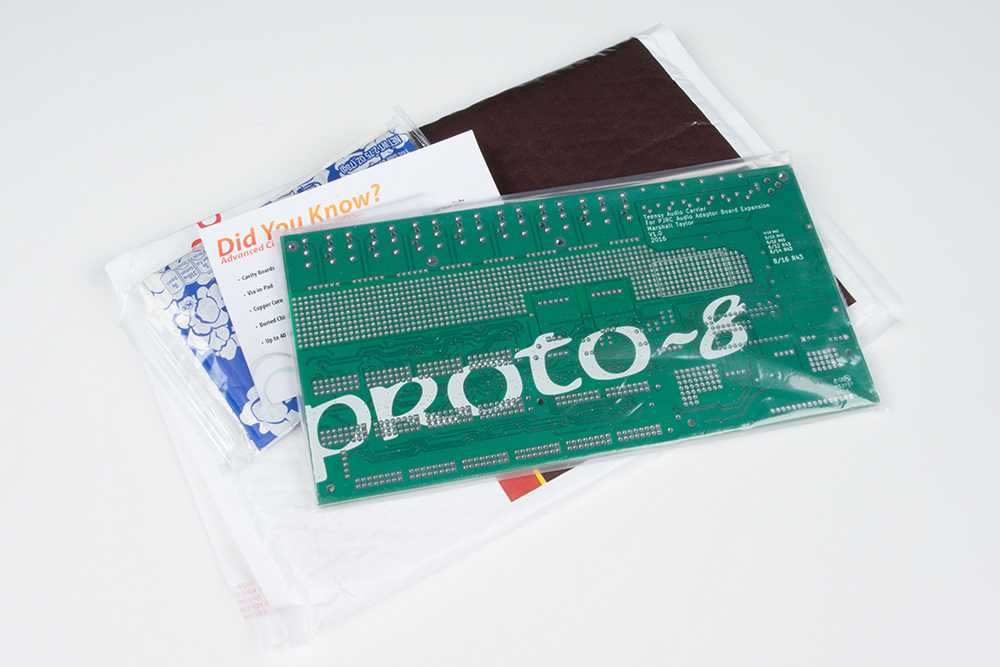
After an anxious week the package arrived!
 |
 |
Shipment from the PCB house. Advanced Circuits sends some complimentary popcorn, which I will consume with a movie next weekend now that the stress of building such a big board is subsiding. Nice! Thanks, Advanced Circuits!
Bring Up the Prototype
Bringing up a board is probably a post on its own, but I have to say something about it. I didn't just load all the components up and apply power. That would be a sure way to get the smoke out. I assembled it in stages, testing between stages. First is the regulators, then the Teensy. Next, the QFN was reflowed and the audio systems tested. Lastly, the IO logic was applied.
Finally, I have access to the black box.
You Can Do It!
I started this project simply because I wanted to try the interactive router. After pushing some traces around I decided to expand the test and try a new PCB service, and the whole project exploded into what it is here.
My basic approach to learning was to watch long, dry tutorials on YouTube. I found a good method was to put them on my second monitor and let them play as I was doing tasks such as building components, researching designs and checking references. Ya know, engineer-y stuff. This gave me a cursory knowledge of what was in the long tutorials. Later, when I needed to do a new task (like working with polygons), I could recall where that information was covered and re-watch the part of the video that was relevant.
Here's some of the videos I found useful:
- KiCad Interactive Router (release version)
- Introduction and KiCad Project Creation
- Creating Power and Ground Planes In KiCad
- KiCad Tutorial #6: Create PCB footprint component
Basically, Anything by Chris of Contextual Electronics, or Tom W, is loaded with good information.
Good luck, and have fun!


Thanks for mentioning CE! I don't usually expect to see too much KiCad on Sparkfun's site, just because I know EAGLE is so integral to the design flow of the SF products, but it's good to show there are lots of options out there (including outside of those two, as well!).
No problem at all. Thanks for making the videos!
Advanced Circuits is one of the more expensive PCB manufacturers. There's a price comparison site, PCBShopper; you enter your board's specs and it shows you prices and delivery times from 26 different PCB manufacturers, including the best-known companies in Asia, North America and Europe (Advanced Circuits is one of the companies listed).
Yes they are expensive, but they're local to Colorado and their quality is quite high. They also do single-board runs for a prototype if you're a college student.
PCBShopper is fun! Thanks!
I didn't worry about the price too much. Even though I paid out of pocket, I consider it an NRE cost to the product I wanted, where the hardware and software design time is massive in comparison. If I was going to go to production though, or order more then a few, I'll have to look into it.
I was extremely satisfied by the quality though, as sgrace pointed out. I'm happy to have my money go to someone I can trust.
Advanced is SUPER reliable. I have never had an issue with their work. If there is a problem or a hint of one they try to let you know. Other shops just run your board however you send it even if it's an honest mistake.
any chance you could put the kicad files on github?
Alright, the github is https://github.com/marshalltaylorSFE/Proto-8
In it you'll find a snapshot of the local directory I was using for development, including the libraries, which are only complete to this project (I haven't put all our libraries into kicad format, just the ones I needed).
Absolutely, but not yet. I just got the hardware up and wanted to log the fixes and create documentation first. This post was about the process but later, there will be another regarding the function and I'll have a package for people to download. Stay tuned!
Awesome. I haven't used kicad before but ... I plan to use Kicad to layout a board with a teensy for a bluetooth project. Looking over another example would really help.
Advanced Circuits is awesome! I remember using them in college, and my teammates and I always saved the popcorn for a late night spent debugging the newly arrived PCB. We used their EDA software (PCB Artist), which worked well and was relatively easy for beginners.
And like sgrace said, they'll do a single board for a college student (we just told them in the comments when we submitted the order). Which is crazy awesome.
For anyone comparing Eagle to KiCad, you should know that a number of professional EDA tools separate component and footprint symbols, and having you sync the schematic and layout manually. This can be tricky, but it's nice because you can have one part associated with multiple footprints, and then choose which footprint to use in the layout. My workplace uses Altium Designer, which works very similarly but is much more complex.
Sparkfun, how many of you use KiCad? Are you switching away from Eagle, or just trying it out?
I'm just trying it out for now -- the learning curve is steeper. I'm going to continue using it for personal projects though, and if any of those projects were accepted to be sold at sparkfun.... what then? Stay posted.
When I first learned PCB Layout it was on OrCAD EDA (MS-DOS version). In OrCAD library management was similar to KiCad and what you describe from Altium, different libraries for schematic parts and footprints. Not only does it allow one part to have multiple footprints, but you can have one footprint that is suitable for many parts.
Granted, at that time that sort of separation was actually better integrated than where we were before OrCAD EDA. We used a program called Schema for our schematic capture and Racal/Redac CadStar for layout. One of the programmers wrote a program to convert the netlist from Schema to CadStar. Because it was so easy to accidentally delete an entire net in CadStar, when we had a first run of boards we would insist on getting photo-plots from the board house before we would let them press any prepreg. Then 3 of us would get together at a conference table and manually compare the netlist printout to the schematic and photocopies of the photo-plots.
Ahhh... The good old days...
I'm glad to see KiCad getting exposure on SparkFun. I've been using KiCad for about a year now and plan on to keep using it. I was using Orcad before, and switching away from WinXP had to find something new. This was an easy transition, or about as easy as any go!. I hope it gets more support from Sparkfun users as time goes on. Another PCB house to try is Accutrace, they offer $3 pcbs if your within their specs. But you to buy 10, still a good deal. Of course they're over seas, so expect a couple of weeks for delivery.
Cool! Thanks for the lead.
I've tried KiCad before and had some problems, but this time around it feels a lot more polished. I hope they keep on developing.
Great to see KICAD on here! It has really gone under steady improvement for a long time thanks to the diligent and dedicated contributors, team, and leadership. It really has a great team of people from all around the world working to make it better with each release bringing new features and bug fixes. More help can be found on their freenode IRC channel #kicad (some devs even hang out there and I have found to be extremely helpful) , Chris Gammell's kicad.info, and their mailing list (not necessarily a place for help, mainly for the devs, but I just lurk on there to check out what new things are in the pipe).
Out of curiosity, what version of KiCad did you use? There is a deserved reputation for stable builds not being available in installation package, but that has changed recently.
In the latest stable version (v4.0.1) and probably several versions up to it, there are alternate methods of specifying footprints instead of using CvPCB. When editing a component in the the schematic (not the library, but a placed component, press the E key when hovering over the part) there is a list of meta-data fields. One of those fields is the footprint field. This is where CvPCB will put the footprints (if you back-annotate from the netlist once you process with CvPCB, which you should do so you don't loose footprints after updating netlist from an iterative schematic change). But, if you select that field in EESchema the button under the Field Value entry box changes to "Assign Footprint". Clicking this brings up the footprint/module library browser where you can select a footprint. Then when you copy that component around the footprint meta-data will also be copied. AFAIK this footprint field can be already populated when designing a schematic library part. So once you as a designer have your schematic libraries and pcb footprints/modules figured out you can assign a default footprint to your schematic parts.
That said, CvPCB is still a good tool for assigning the same footprint to lots of parts, and double-checking to see if there are any parts that haven't been assigned a footprint yet.
I've also had good luck importing Eagle footprints into PcbNew. Just last night I downloaded some Eagle footprints from Newark/Element14 and used the footprint library wizard to add them as project specific libraries. (Ok, just the .lbr library... I had to install Eagle to convert the .scr scripts to a .lbr library, but that worked well.) I could have added them as global libraries, but I'll probably copy the imported footprints to my personal libraries once I've vetted them, or decide against that and just use footprints that I generate using an IPC calculator...
I'm using 4.01-stable on windows. I did notice that the field got populated after running CVPCB, I never considered that it could have been entered at schematic time, but sure enough it can! I'm not sure which way I like better though. I think the CvPCB method makes more sense because the work can be done in batches, but I donno, I might use the properties in some situations.
I had some luck importing Eagle footprints as well, but I can't remember what I used to do it. There seems to be quite a few tools people are putting together and I'd like to test drive some of them, especially for converting whole designs back and forth, and not just the libraries. I'm saving that project for another day though.
Thanks for the comment. I found previous versions too buggy to use, but this time I was really impressed. Maybe I should have been compiling them myself!
One trick that I've tried (as a test, but not in actual design mode yet) is to assign a footprint to one part (preferably the first ref'd of many) in the schematic. Then when in CvPcb, click on the one that has the footprint and it is found in the big-huge-list-of-footprints.
Also, there is (limited) connection between the schematic and pcb. If you have both EESchema and Pcbnew open when you click on a component in one your pointer in the other snaps to it. Useful for when you can't find C231 on the schematic but know where it is on the PCB. (And vice versa.) Dual monitor setups are useful for trying this. (AFAIK, I think that same link is there between EESchema and CvPcb.)
Check out the three videos on the KiCad web site for Pcbnew for the new features added to Pcbnew: http://kicad.org/discover/pcbnew/ According to the KiCad/CERN roadmap(s) many of the changes being developed (and end-user beta tested) in Pcbnew should eventually make their way to EESchema. Also, the missing editing features in the OpenGL canvas in Pcbnew should eventually make it there at which point I think the plan is to depreciate the current default canvas. (Something I noticed last night, the markers for Pcbnew DRC errors don't show in the OpenGL canvas...)
I think if you had been compiling the BZR nightlies yourself, you would have gotten really frustrated if trying to use it for production. Just about every new feature was a moving target. It took me a while to figure out what was going on when the new footprint library tables were instituted, as the documentation was essentially everyone on the KiCad mailing list trying to figure it out together... Documentation always lags development...
Hi Sembazuru! We've been talking in the SparkFun forums about the links to the old domain. Do you think you can update the link in your comment as well?
Thanks! ;)
Fixed. Thanx!
I like that technique! I agree, with the millions of parts they're hard to find sometimes. The other think I've found to do is to use the suggested footprint name feature during library creation, so I can filter by the names I've specified.
I noticed the cross-linking, but It didn't seem polished enough to be too useful yet. My fingers are crossed.
Thanks for the links, I'll check them out.