Enginursday: Sparking Creativity in Troubleshooting
Let's talk about a PCB design error and troubleshooting the root cause.

My prototype PCB design came in and is all built up and is ready for testing. I connect the board to my PC, but sadly, no signs of life. I measure the resistance between the supply voltage rail and ground, and I get 0 ohms. Hmmm well that's not ideal, let's see what's going on.
The way we build prototypes here at SparkFun is we order a few PCBs and a solder paste stencil, and then hand place the components before reflowing the board to melt the paste. Prototypes allow us to not only test the PCB design, but also to test our paste stencils and make sure we're not adding too much solder (which could short components or pins together), or too little (which could prevent a part from making a secure electrical/mechanical connection).
The design has a new QFN part with an exposed pad underneath, which is connected to ground. My first thought was the stencil used too much paste and the paste is shorting my 5V rail to ground. I de-soldered the part, wicked off as much solder as I could and did a visual inspection to make sure I couldn't see any problems. I took another resistance measurement, and still, 0 ohms.
I pulled up the design and removed every part that was connected to the 5V rail, but still, 0 ohms. I grabbed one of the extra boards that wasn't populated and measured the resistance, and even the blank board has a short. I started to do a visual inspection of the board, looking for problems like this:
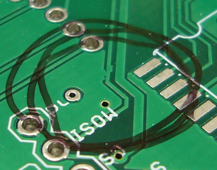
I looked over both sides of the board, without finding anything. This is a four-layer board though, and most of the copper for the 5V rail is on the inner layers. I checked the design again, and looked at the Gerber files to see if it was a design error or a manufacturing error.
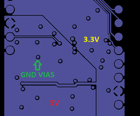
On layer two, I have my 5V and 3.3V power rails, and on layer three I have my ground, using vias to bring power and ground to the top and bottom layers. The only thing I can think of is a whisker shorting to a ground via from the inner layer. Without specialized equipment like an X-ray, I can't do a visual inspection, so how can I test that?
POWER!
If you think of how a fuse works, you have a large amount of current passing through a wire. As you increase the current, the wire starts to heat up; add too much heat, and the wire melts and becomes an open circuit. Ideally, I'd like to be able to still use the boards if it's a single whisker, so I connected our 20A Mean Well power supply. One hundred watts should be enough right? Maybe, but the short circuit protection of the supply works too well, and I wasn't able to make any sparks.
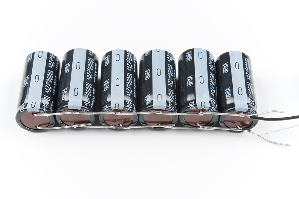
Since it's the current that I need, I soldered together six 10,000uF/25V in parallel to create a 60,000uF short finder. After charging the capacitor bank to 5V I connect the leads to 5V and ground, keeping the wires short to minimize power loss in the cables. After a small spark, I measured the resistance again and this time I saw ~1MΩ. It's not perfect, but it should be good enough.
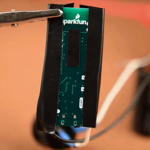
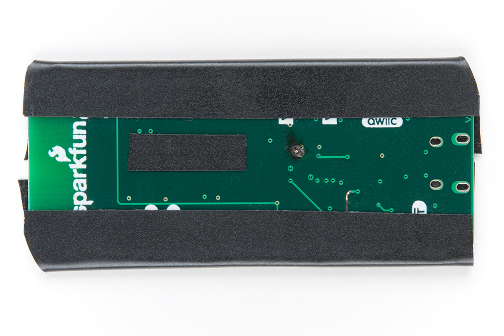
Because we have a few copies of the board, I was able to film clearing the short. The first time however was a bit more dramatic, with a small flame of 2-3mm in size, that burned itself out pretty quickly, but it made it obvious where the short was, as seen below.


I often (well, not TOO often) use a somewhat similar method, but rather than trying to blow the 'fuse' I search for the hot spot. I use a current limited power supply and slowly ramp up the current. Occasionally this is enough to blow the unwanted 'fuse', but for harder shorts I go looking for heat. If I am feeling brave this is done using a uni-pixel thermal scanning sensor (my finger). For more complex boards, or boards with components on both side where the mono-scanner can't pass smoothly I use a thermal camera. This also works for circuits with faulty components and/or incorrectly connected components. Proved very useful on one particular design when I updated an ADC to a higher performance ADC in the same family/package only to discover one of the ground connections had been re-tasked as a power supply. The updated ADC shorted the power internally. Once discovered simply lifting the rogue leg fixed the issue.
Sounds to me like a good use for the FLiR kit or the older version that SparkFun sells. Fortunately I haven't had to chase a power short in a PCB since I purchased the older version more than 3 years ago.
Back in the "dark ages" (before FLiR cameras), one very tedious approach to finding shorts in a PCB was to use an ohm meter that used a "Kelvin" (4-wire) connection rather than the more common 2-wire connection. These meters can get down into the sub-milliohm range, and get you "closer" to the short. Unfortunately, these meters can be fairly pricey (think a few thousand dollars) and require a very high skill level. For this sort of use, though, calibration isn't critical (as long as the meter is stable enough to not "drift" over a few hours/days of use), so sometimes you can get lucky and pick up one used but not calibrated for a decade or more for a much more reasonable price (think hundreds of dollars). Getting one calibrated can cost hundreds of dollars, not to mention the round-trip shipping.
I see not just a burn mark, but a board with its identifying marks masked off. I shiver with anticipation!
(I know that companies prototype stuff all the time, and many products are dead ends. Which is why early prototypes are not revealed without masking.)
Car batteries are not anywhere near current limited for an application like this :)
For over ten years I have been using a variation on the four terminal Kelvin resistance measurement to find shorts on pc boards. I use a one or two amp current limited low voltage source. This could be a 5 volt supply with a four ohm power resistor or a lab supply set to 3 volts and 1 amp. I connect the current source to the two shorted traces at easy access points, usually by tack-soldering short scrap wires to components or connector pins on the problem foils. Then I set a DVM to read volts with resolution to millivolts and start measuring voltage along the foils. You may start out with 30 or 40 millivolts. Work your way along the traces to where the voltage goes to zero or a minimum and you are at the short. If you have a ten ohm tin whisker between two foils, pass the current thru one of the foils from one end to the other. Treat the foil with current as a voltage divider and the other foil as the wiper on a trimpot. At the place where the voltage on the current foil equals the other foil you have the short. I have used this to find whiskers that were barely visible with a microscope. A small scratch with an xacto blade cleared the short. Four terminal resistors and voltage dividers are handy tools!
And if you contact the board manufacture and show them the manufacturing defect the response will be "well you didn't pay for electrical test so too bad". It's only happened to me twice so far and since they were prototypes it was just an inconvenience not a money looser.
I had a board like that, where I had lifted some of the circuitry from an open-source product. Eagle told me there was an issue there, but it was a working board, so I approved it and sent it off to fab. Sure enough +3.3V was shorted to ground: right in that borrowed layout. It took a little while to narrow it down, cutting traces here and there and using a short tracer. The next revision, I paid more attention to the DRC errors!
Back when I was a test technician in the 70's, we would do the same thing with boards that were 20" x 30", all DIP logic, with power typically +24, +/-15, +12, and 5. I believe the power supply I used was 50amp (Big Bertha) and if we got a pop with no burning, the board went on to chamber testing and burn-in. If the PCB was burned then it became an internal reference board, can't ship those to customers.
Well yeah, but I had one burn along a path of an internal run for about 9". How big are those stickers? :-)
When I was a factory tech back in the mid-70s, I was mostly working on thick film hybrids (circuits literally printed on a ceramic substrate -- a low resistivity ink was used for conductors, and higher ones for resistors which were later laser trimmed to be "in-spec"). The largest was about 2"x2", and when we had a lot of trouble finding the problem, we could occasionally get away with the "waffle test" -- place the board on the floor and firmly apply the "waffle-stomper" (aka hiking boot). Always solved the problem... ;-)