Creating an RF Shield
Any FCC certified module needs a tin can to protect and prevent RF emissions. Check out how we did it for Artemis!

For years, SparkFun was wary of getting a product fully FCC certified. The process always seemed unknown and prohibitively expensive. We've written about the FCC requirements for products and hobby projects in the past, but with the development of the SparkFun Edge and the creation of Artemis it was time to venture into uncharted territory. We hope you can learn a little something from us. This is a three part series covering the creation of the Artemis SMD module, getting an RF shield made (twice), the FCC certification process, and porting Arduino.
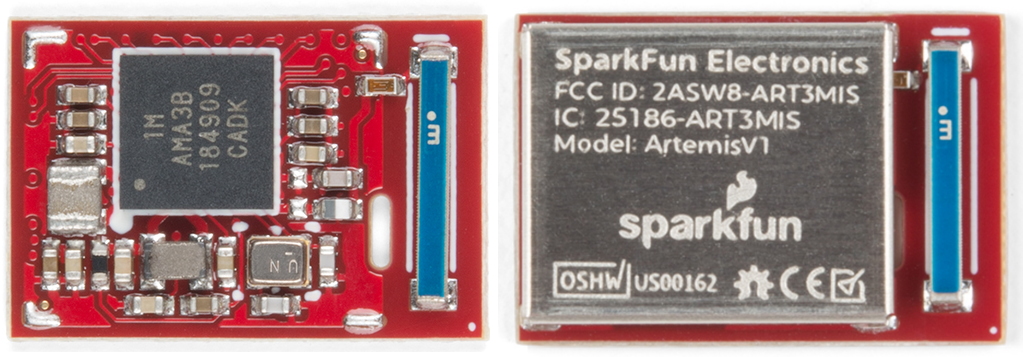
Now that Artemis was designed and working, it was time to begin the FCC certification process. One of the requirements for FCC approval is RF shielding for intentional radiators. In other words, if your thing does wireless it needs a metal 'can' over the top of the design to reduce the amount of spurious RF noise. Additionally, the shield protects against incoming RF radiation from other devices. I knew Artemis would need a metal stamped shield, but how would we design one and get them made? A quick search on Alibaba turned up hundreds of potential suppliers. After cold contacting a few of them it was clear that having a shield was straightforward, so I started feeling out what they would need. Could they design the can for me, or did I need to provide a full 3D drawing? I naively thought I could give my PCB design to a sheet metal house and all would go well. As with any custom product, a clear spec is what is needed; it was time to model the shield in 3D.
As an EE I have neglected to jump on the 3D CAD/printing bandwagon, so I resorted to my old friend Sketchup. Don't laugh, I really don’t do 3D modeling...
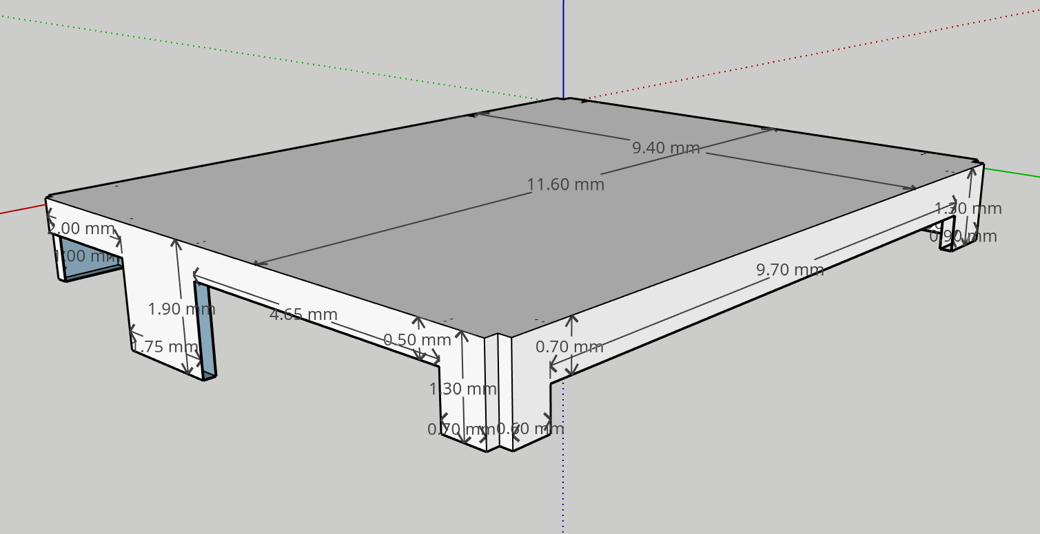
Original RF shield showing dimensions in Sketchup
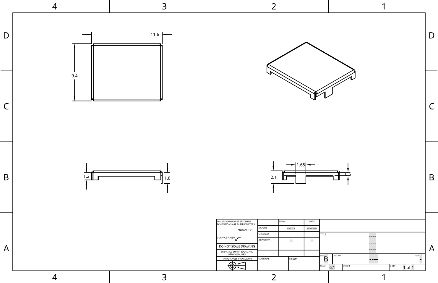
I knew from taking apart other modules that an alignment leg was a good thing. The alignment leg is slightly longer than all the other 'legs' of the shield and protrudes into the PCB, but stops before coming out the bottom of the PCB. This would allow the pick and place machines to place the shield confidently, as long as the alignment leg was dropped into place. I also knew the approximate thickness and bend radius from measuring shields of various modules I had laying around.
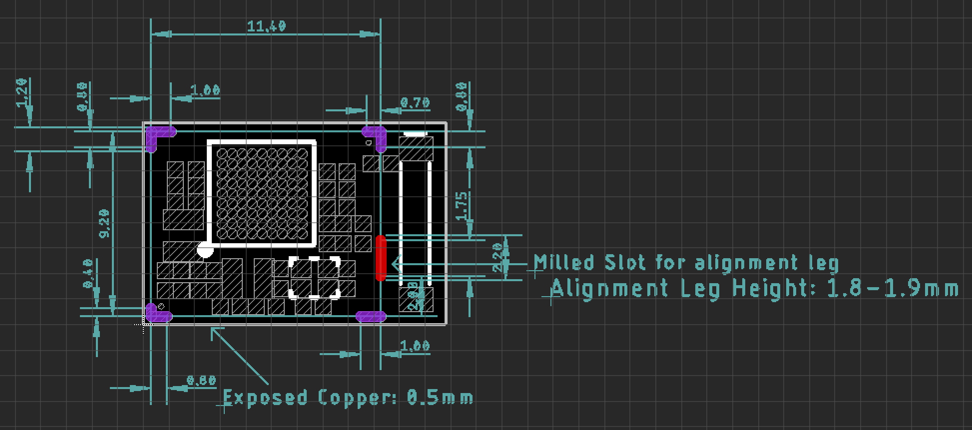
I added a few SMD 'landing' pads (again, modeled from other SMD modules) to the Artemis PCB and then designed a shield to match those pads.
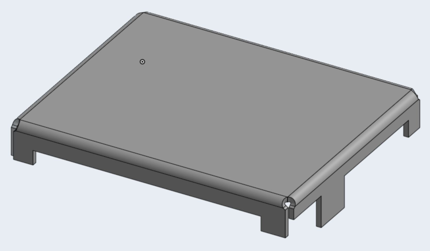
Artemis RF shield designed in OnShape
I had my design in 3D glory but the manufacturers started asking for a STEP file, a common CAD file format that SketchUp doesn't natively output. Rather than try to fit a square peg in a round hole I decided to switch to OnShape, which is a parametric based 3D modeling program, and very capable of outputting the file formats the stamping companies were used to working with. Additionally, since stamped metal parts are very common, OnShape even had a built-in tool for creating stamped and bent metal parts, making the creation of the shield that much more true to life. And finally, it’s free for publicly-shared projects (OSHW for the win!).

Side view of Artemis showing air gap
In my survey of various modules there is often an air gap between the PCB and the shield. This serves two purposes:
- Thermal escapement. If the RF device generates heat, these gaps allow a certain amount of airflow. In the case of Artemis, the power consumption is so incredibly low (less than 0.5mA at 48MHz) that this was not a main concern.
- Reduction of PCB landing space. We could ostensibly solder 100 percent of each side of the shield to the PCB. The landing pads would be very large. By making smaller islands, we can still route some traces under the air gaps.
Thus, my RF shield had a few small landing pads. In addition I did a quick datasheet check on all the SMD components’ dimensions that make up the Apollo3 support circuitry. I needed to be sure that the overall height of the shield would be tall enough not to collide with any of the underlying components. There was one inductor on the original Edge design that needed to be swapped out for a shorter, equivalent inductor. If I were a 3D guru, modeling the PCB and components in real time with the RF shield would have been illustrative but in my case, unnecessary.
After a bit of floundering and a few videos showing how to create metal stamped parts, I was able to create the RF shield in OnShape and produce the necessary files for a few manufactures to generate quotes (also known as RFQs). What I got back was promising. It was approximately $600-$1600 for tooling, and a piece price of $0.10 to $0.20 per unit. A few manufacturers could not do tape-and-reel packaging so they were removed from the running. One manufacturer offered free laser etching with T&R for $0.10. Pretty amazing.
What really struck me during this phase was that I was just trying new things without the knowledge that it would work! The guesses were educated but I was supremely lucky in the end; everything worked out on the first try. Well, at least the shield fit the PCB perfectly...
A few emails were exchanged, including the question of what metal we required. Serendipitously they asked and answered their own question (suppliers like this are hard to find!):
2.Do you have specific material requirement?
Usually, About the choice of materials, there are 3 types main materials for manufacture Metal shield: Nickel Silver (generally preferred), Tinplate and Stainless steel, and usually will not need do surface finish on them.
1) Nickel Silver and Tinplate can be soldered, but Stainless steel material can't be soldered.
2) Nickel Silver can be oxidized, but not easy to rust. Tinplate is easy to oxidize and rust. Stainless steel can't be oxidized and rusted.
3) Nickel Silver's price is highest, Tinplate's price is lowest.
4) Nickel silver and Tinplate are 2 types main material for manufacture 1-part Metal shield; And the main material for 2-part Metal shield: Shield Cover (Stainless steel or Nickel Silver) + Shield Frame (Tinplate or Nickel silver). But for 1-part Metal shield, our factory usually recommend Nickel Silver to our most of customers. What do you think of it?
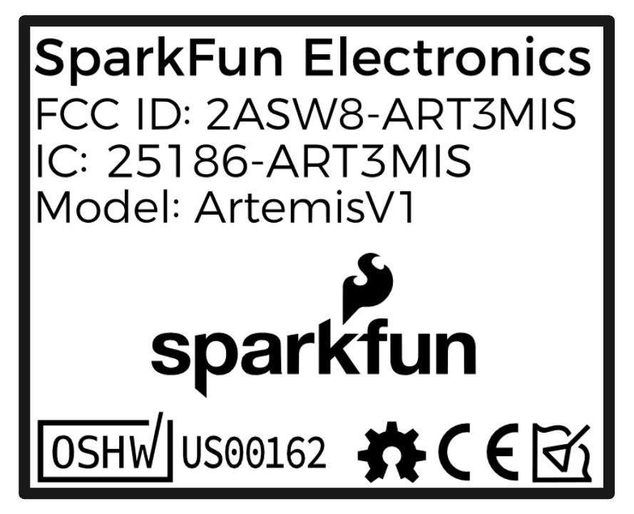
Nickel silver it is! The next design step was the labeling on the shield. The FCC requires the label design to be submitted as part of the product’s application. So while you don’t have to have a picture of a final unit (a Photoshop mock up is acceptable) you better not be changing the layout once you go to market. There are a few ways to do this:
Sticker vs Etching vs Stamped Logo
- Sticker: Allows the end manufacturer (SparkFun) to print the label and any custom identifying features such as MAC addresses or unique serial numbers. Great, but I didn’t want to deal with tens of thousands of labels being manually applied to each Artemis.
- Laser Etching: Obviously a lot more permanent than a sticker but unique IDs becomes problematic.
- Stamping: Cheap! But generally not detailed enough for small fonts. The Artemis shield is less than 10x15 mm, so we needed really high resolution.

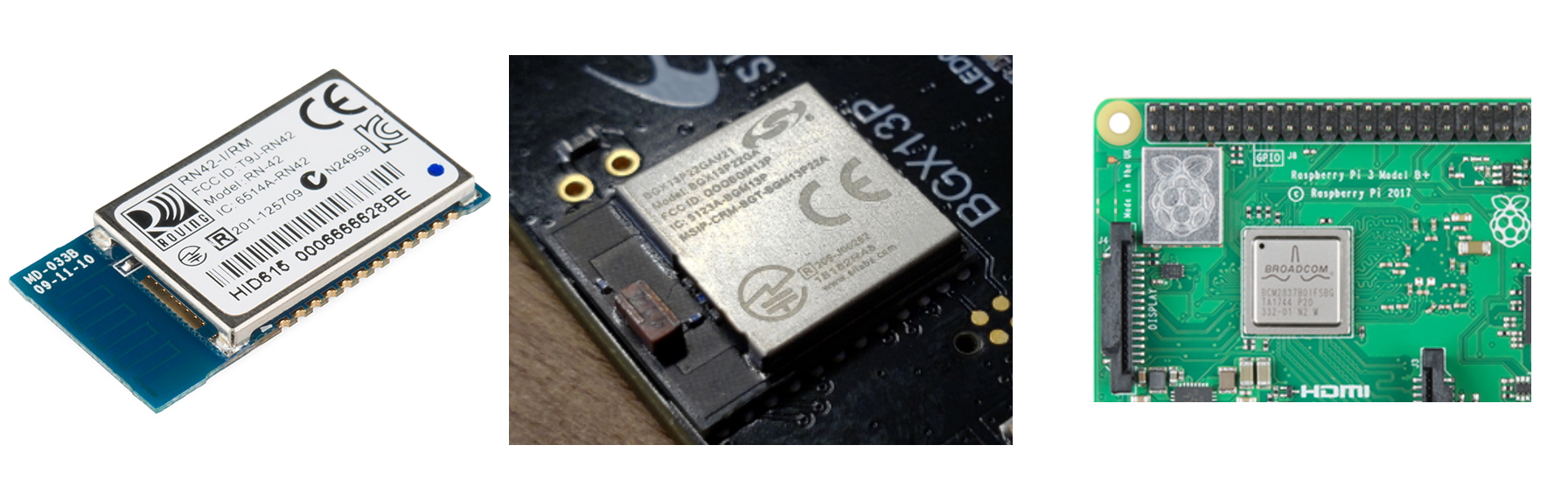
After researching various RF shields I began to scratch my head at the iconography and data included on each shield. There’s the obvious FCC ID, but a variety of shields had a variety of additional markings. I determined that Model is generally used by the manufacturer (in this case SparkFun) to tell the user what the thing is. Then there’s an IC mark that seemed to be generated by the company, like a sub-model mark (for example an Apollo2 based Artemis vs and Apollo3 based Artemis). Then there’s a bunch of various logos and icons. What to do?
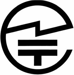
After a bit of searching we identified the above icon as the Japanese Ministry of Internal Affairs and Communication (MIC for short). If a device has this marking it’s been specifically tested and approved for use in Japan. Since we didn’t want to pay for testing in Japan (yet) we refrained from adding this icon to the shield.

Onion Omega2 module with CE marking
CE is a mark indicating the module has passed the preliminary testing required for a product to be certified in Europe.

nRF52840 module with CMIIT marking
CMIIT is the Chinese Ministry of Industry and Information Technology. Since we didn’t plan to certify Artemis in China, we skipped this icon as well.
In addition, from our contact at our test facility:
"Don't put the FCC logo on the shield. It really annoys them."
So taking all that into account here's our first design:
Artemis etch design v1
After approximately 62 emails back and forth we had an inbound shipment of seven tape-and-reels of 1500 pieces per reel.

Tape-and-reels ready to ship
A few weeks later the shields arrived and we built up a few units of Artemis using these new, fancy looking RF shield. I was immensely relieved everything fit! No component collisions, the alignment leg fit great. Our pick-and-place machines could pick this rather large part without issue. I was overjoyed that the shields were working.
At approximately the same time, the blank Artemis module was going through lab testing. Around this time the company we were using for FCC testing began asking us for the shield's graphics so it could be included with the application. They also asked if we had gotten our ISED number from Canada. What's an ISED number? I thought Canada used reciprocity with the FCC. The back of my brain started raising alarms. Within minutes it was obvious that I had confused IC (integrated circuit, in my head) with IC (Industry Canada).
So close! But never to see the light of day...
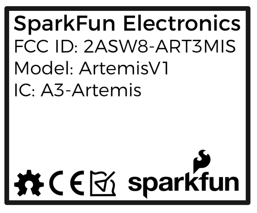
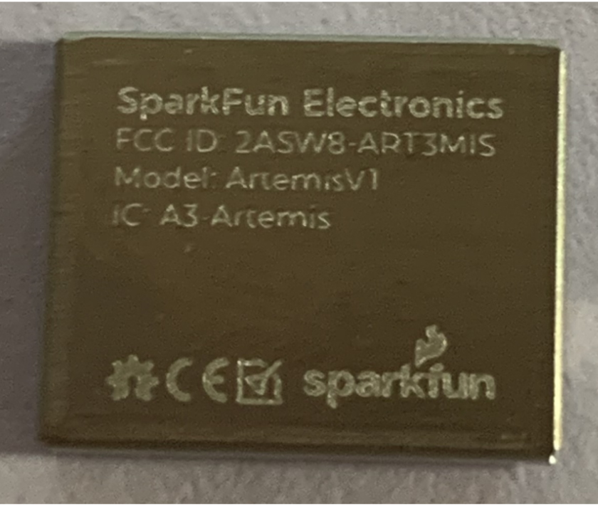
All 10,000 RF shields had the wrong labeling. Ugh! I’m sorry, Earth.
Corrected IC number
We sorted out our ISED certification number and had another batch of shields made. Given the chance, we added our OSHWA certification number and the OSHW logo as well. Since we had already paid for the tooling, this second batch cost only ~$1000, but took an additional five weeks.
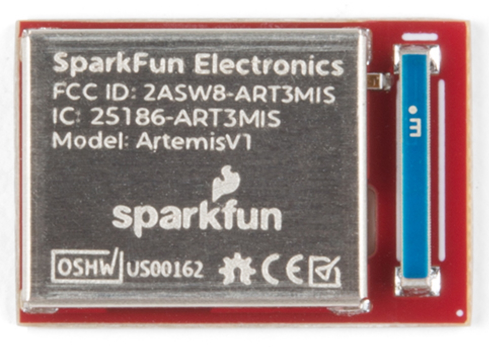
While it was painful to get it wrong, the second version of the etching came out great. We were able to add a few icons and stretch the etching area to the borders of the shield, increasing readability. Remember, this is 10x15 mm - the writing is tiny and every millimeter helps.
Once the shields arrived we could start to produce fully shielded modules. Now all we had to do was pass our FCC testing...


Hi Nate!
Another great post! Looking forward to seeing "Part 3"!
By an interesting coincidence, last night I heard a talk at a local Amateur Radio club from a gentleman who works for a local company that makes "implantable electronics" -- such as pacemakers and neurostimulators. Since these days such gadgets are capable of (wirelessly) communicating with computers outside the body (some of the latest even use Bluetooth), they have to have FCC certification, even though their necessary "communications range" is maybe 2 arms' length (e.g., from patient in bed to bedside stand). However, the FCC stuff is a "piece of cake" compared to getting FDA approval!
One thought that crossed my mind as I was reading your article was that I'm a bit surprised that there aren't at least a few "standard dimension" shields on the market for folks who only need a few, and are willing to "oversize" the shield a bit (to avoid the big bucks of tooling costs). Clearly using these (probably) eliminates the laser marking, but there are other methods for marking. (BTW, the reason that most things get marked on the shields is that it's a convenient place to do so. Last time I went into that swamp, the FCC just required that the "device" be permanently marked somewhere visible -- some folks even use text etched into the "spare copper" on the PCB.) I suspect that there are some "standard cans" that I haven't come across...
Anyway, thanks again, Nate, and Happy Thanksgiving to all the SparkFunions!
I am a RF Engineer developing a commerical product involving a ESP32-PICO-D4. Operating @10dBm, this PCB apparently requires a stamped metal shield to pass FCC. I am very interested in learning the identity of the supplier who worked out so well for you. https://www.zebryk.com/ Jay@Zebryk.com
This is an amazing article!
I glad to see you used the right CE mark (CE Mark vs the China Export Mark). See "https://www.ybw.com/vhf-marine-radio-guide/warning-dont-get-confused-between-the-ce-mark-and-the-china-export-mark-4607".
Hi Nate:
Happy Thanksgiving! Thank you for sharing the awesome details on how you/SparkFun went about getting the right certifications and placing them on the shielding frame. Very insightful.
You had mentioned that you paid approx. around $1k for the second run with the IC # change. Can you give us a ball-park number on how much it costs these days for "an initial tooling"? This will give someone like a hobbyist trying to build something a rough idea of how much some of these start-up costs will be.
Thank you again for taking your time to share all the wonderful details.
Cheers.