Creating Artemis
Learn how we created our own SMD module using PCB tips and tricks for blind and buried vias.

For years SparkFun was wary of getting a product fully FCC certified. The process always seemed unknown and prohibitively expensive. We've written about the FCC requirements for products and hobby projects the past, but with the development of the SparkFun Edge and the creation of Artemis it was clear that it was time to venture into uncharted territory.
We hope you can learn a little something from us. This will be a three-part series covering the creation of the Artemis SMD module, getting an RF shield made (twice), and going through the FCC certification process. Stay tuned for the rest of the series.
Creating Artemis
Back in October 2018, we were introduced to the folks at TensorFlow to do a low-power board with the new Apollo3 from Ambiq. After a quick scan of the datasheet it was obvious this IC was as challenging as it was exciting! One MB of flash, nearly 400k of RAM and exceptionally low power made us start dreaming of the possibilities beyond the old Uno. At the same time, an 81-ball BGA with 0.5mm pitch meant we'd have to up our PCB game.
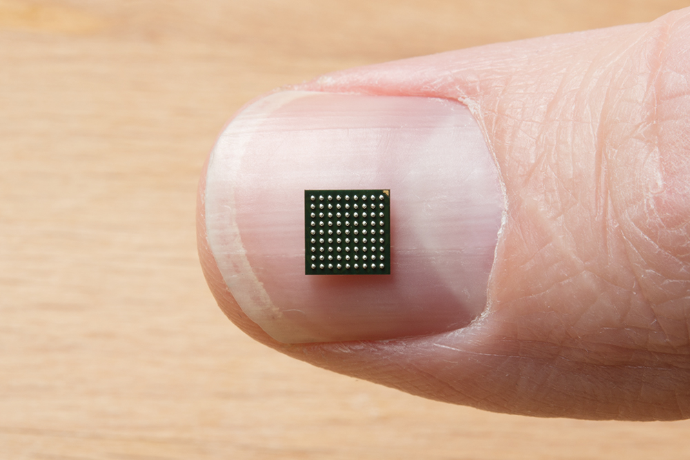
81-Ball Grid Array with 0.5mm pitch
The project was nicknamed SparkFun Edge (the whole computing on the edge thing) and we dove into getting to know this new IC. The Apollo3 is a straightforward microcontroller but the density of the balls made routing a design far more interesting.
The BNO080 breakout is a good example of SparkFun designs.
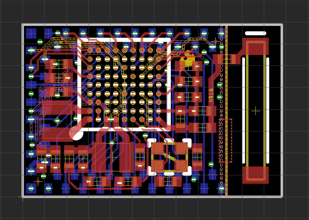
Most SparkFun designs can be done with rather large trace/space requirements (8 mil trace/space) with small-ish vias (12 mil) on two layers. These specs are very common and make for very low cost PCB fabrication. To even begin to route the Apollo3 we reduced the trace thickness to 5 mil, the vias down to 6 mil and used a four layer board, but it was still impossible to get to the inner balls. Let’s talk about some of the challenges and solutions.
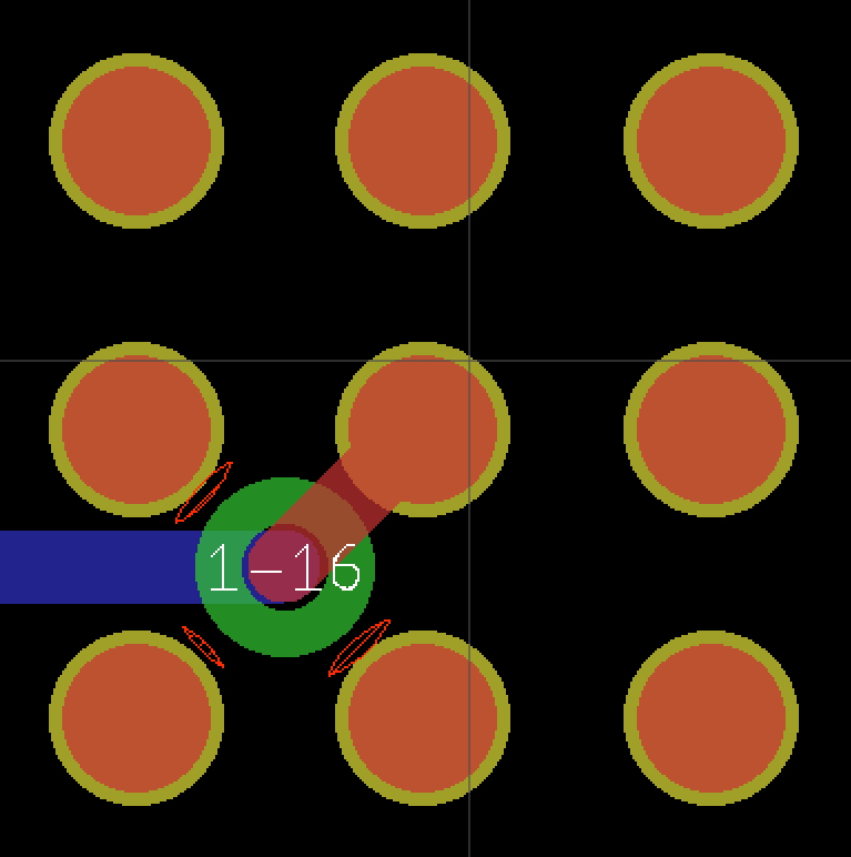
We first started by placing the vias adjacent to the ball. As shown above, the vias were still massive compared to the balls. The annular ring of the via is too close to the neighboring pads, causing DRC errors. Because of the 0.5mm pitch on the Apollo3 we would have to use a 3 mil-sized (0.003”) via in order to not have the annular ring be within 6 mil of a neighboring pad. This sized via is solidly in the territory of expensive laser drilling, which can be prohibitively expensive. So the first PCB trick for 0.5mm pitch BGAs is called via on pad. This is a method to allow the placement of vias directly under a ball.
A via is placed directly on the pad where the ball will be soldered.
Normally, vias are not placed directly on an SMD pad because the solder paste tends to wick down into the hole during reflow, reducing the solder available to the pad and leading to unreliable connections. Fab houses are aware of this so, as an alternative to costly laser drilling, they have developed via-in-pad, which is a succinct term for drilling a very small via, plating the hole, back-filling the hole with conductive epoxy, then plating and polishing the fill so that it forms a flat, solid pad.

On the left you can see the original Edge with its filled vias. Note how the vias appear flat. There are vias inside of many of the BGA dots as well. On the right is the ATECC508A Crypto breakout. You can see the ‘dimples’ on the PCB where the mask dips into the vias. Those vias are empty and cheap to produce.

Trace route blocked by annular rings
Via-in-pad allowed us to route directly down to a lower layer, but again we were foiled because the traces couldn't fit between the vias on adjacent pads. We could get down, but we couldn’t get out. The next trick is blind vias.
Blind vias on the left. Buried vias on the right.
Blind vias basically means vias that don't go through the entire board (they are ‘blind’ to the opposite side of the board). Buried vias are limited to inside layers and do not protrude to the outer layers. These types of vias require the individual layers to be drilled, then precisely aligned and laminated to the next layer, then holes are plated, then the next layer is added and the process is repeated. Euro Circuits has a great writeup of the process and the challenges associated with the different types. While tricky and more expensive to produce, blind and buried vias are often necessary for compact designs such as the Apollo3.
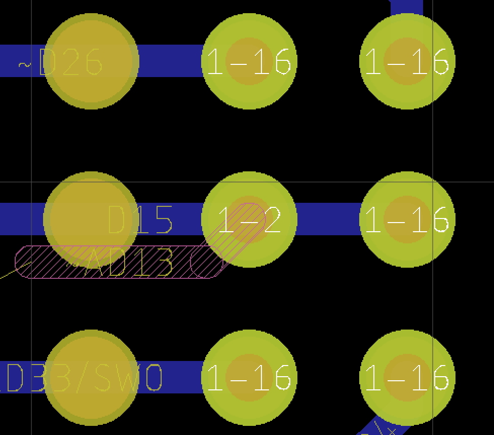
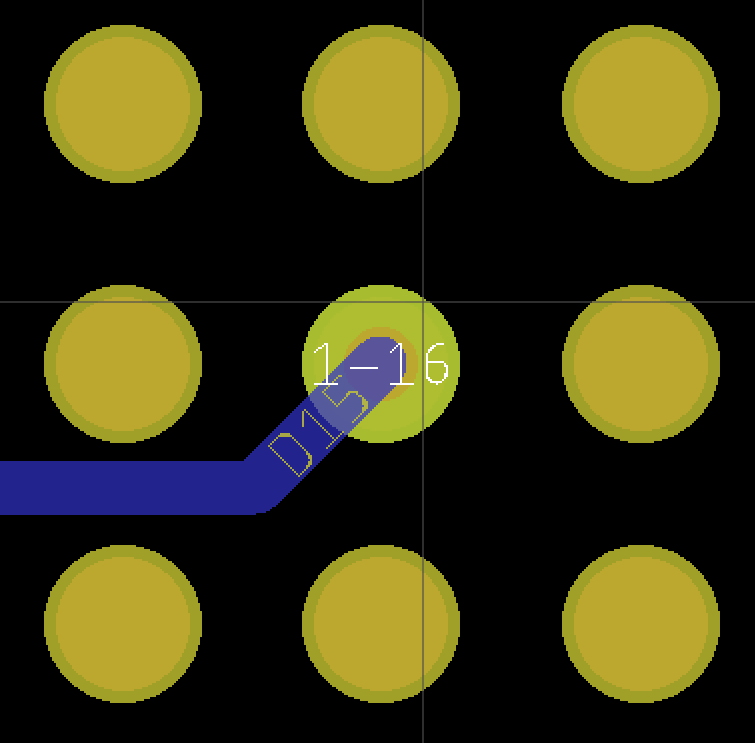
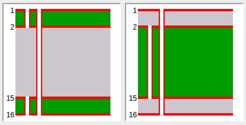
In the above image, Eagle shows which layers are connected by the via with text on the via. One-two means layers 1 and 2 are connected. One-16 means layers 1-2-15-16 are connected.
It’s a bit trippy the first time you do it, but you can see in the above image the AD13 trace has a via going from layer 1 to 2 (blind) and continues on layer 2 (mid layer pink-ish). The D15 trace has a via that goes from layer 1 to 16 (through) and continues on layer 16 (bottom layer blue). Using blind vias, we can finally begin to route out the inner balls to the rest of the circuit.
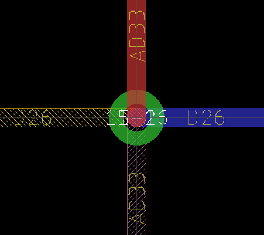
It gets even weirder when you have vias on vias. Shown above, there are two vias on top of each other. We have AD33 coming in from the top of the image (red) and going into a 1-2 via and exiting the bottom of the image (pink-ish). D26 enters from the right of the image (blue), goes into a 15-16 via and exits the left of the image (yellow). Because the vias are blind (and are insulated by the core FR4), they can be stacked on top of each other.
After much tweaking and price checking, we used the following specs to route the Edge:
- Min Trace Size: 0.004” (0.1mm)
- Min Drill: 0.006” (0.15mm)
- Annular Ring: 3 mil
- Min Trace to Pad Spacing: 4 mil
Can PCB fab houses go smaller than this? Certainly, but the costs go up exponentially. Let’s call the above numbers “very tight” PCB specs, and they cost a lot more than the very low cost PCBs that are available from the likes of PCBWay, PCBUniverse, JLCPCB, etc. Over time these specs will probably get even better for cheaper, but today, this seems to be the soft spot right before the “ludicrous” specs of laser drilling, 6+ layer stackups, and a combination of buried and blind vias.
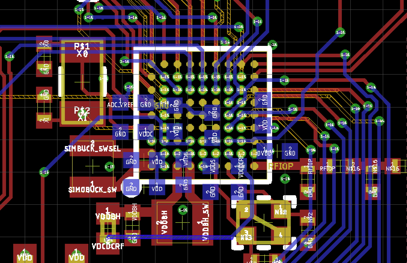
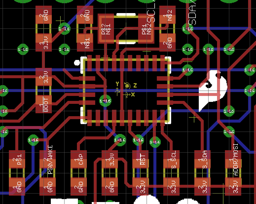
The routing in and around the Apollo3 IC on the SparkFun Edge
Once all these advanced techniques were enabled within Eagle, the routing of the Edge proceeded like any other design but with a lot more staring. It's amazing how foreign viewing four layers with not-through-vias felt and how, after two days of futzing around (and dreaming of vias), the brain remaps a bit and it gets easier to see how things are connected. While these methods are common in High Density Interconnect (HDI) PCBs that make up a huge chunk of modern electronics, this type of routing and PCB design was new and exciting at SparkFun.
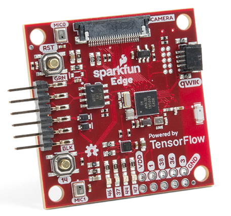
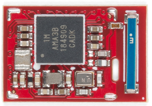
The SparkFun Edge with Apollo3
We were able to deliver the Edge on time and (nearly) on budget for Google's TensorFlow conference. What pained me was that we needed the "very tight" specs for a few square millimeters around the Apollo3; the rest of the board was trivial and could be routed with regular 8 mil trace/space but (of course) we had to pay for the entire PCB. The Edge is relatively large, so the cost of PCB rivaled the cost of the main IC. In addition, the lead time for this type of advanced PCB meant the Edge would suffer from long lead times due to the boards taking time to fabricate. Any changes we wanted to make to the PCB would cost many months and hundreds of dollars to test.
But what if we could create an SMD module that had the Apollo3 inside? We could move all the complexity of the crazy back-filled blind vias and four-layer routing into a smaller module that (hopefully) would stay static. We could simply plop this "known good" block onto a design and not have to worry about PCB lead times. The Edge could move to a two-layer PCB, making it far easier to revise and add features. We could even design additional carrier boards for this "known good" Apollo3 block. And wait, couldn't we sell this module to other companies so they could use the Apollo3 as well? Oh! And…
The ideas kept coming. It was obvious we needed to design a compact SMD module, deal with RF shielding, go through FCC and port the entire Arduino core over to the Apollo3. Just a few challenges! But all new and exciting ones.
How to Design an SMD Module
Don't forget that Artemis is an open source hardware design. You can download the Eagle files here and checkout and even modify the design yourself!
The internal layout of Artemis
To create the Artemis, we were lucky to start from a known good design, the SparkFun Edge. We knew how to wire the Apollo3 and make it work. Now we just had to compact it into a one-sided board. We first started by looking at all the SMD modules we could find.
The pads on most SMD modules can be grouped into two basic groups: castellated and buried.
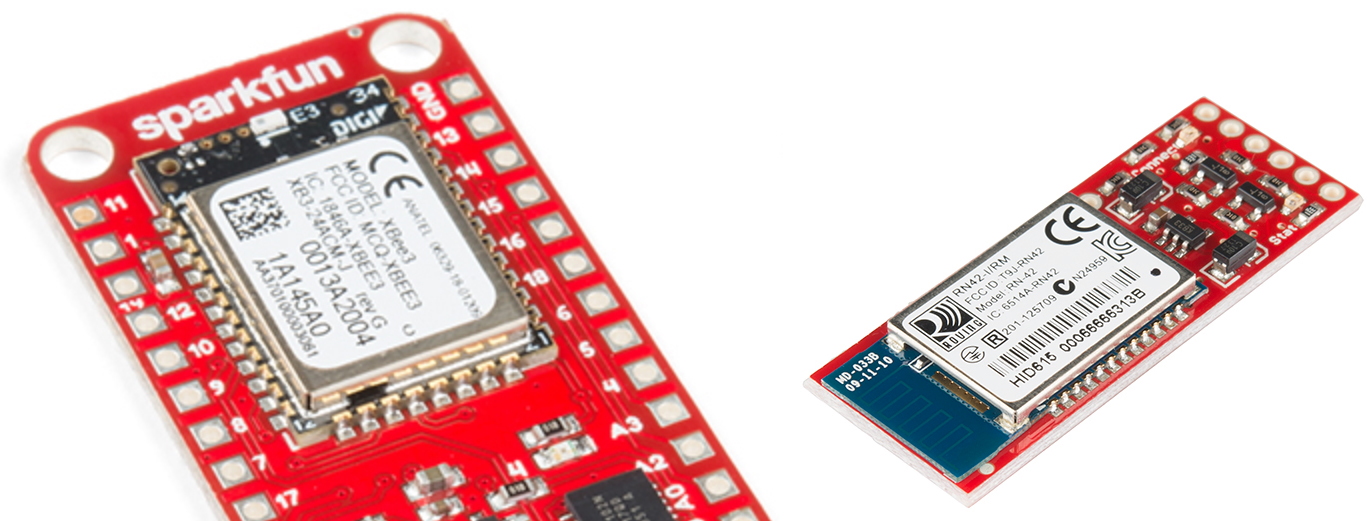
Two modules with castellated pins: Thing Plus - XBee3 on left, BlueSMiRF on the right.
Castellated pads are easy to solder and easy to inspect. The problem is that you're really limited by the number of pads you can expose. On a module with an onboard antenna, you’re limited to three edges. In most modules it's a dozen, perhaps 20 pins that are exposed to the user.
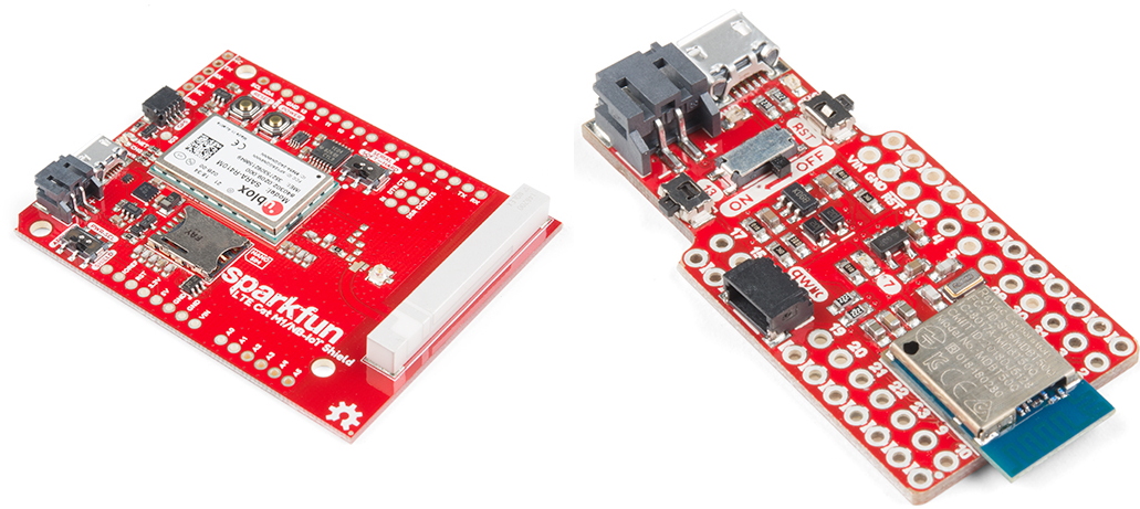
Two modules with buried pins: SparkFun NB-IoT Shield on left, nRF52840 Mini Breakout on the right.
Buried pads are located under the module and cannot be seen from the top or sides of the module. These types of pads would be harder for the end user to inspect and rework, but it dramatically increased the number of GPIOs and features we could breakout of the Apollo3. Buried pads are not new or even necessarily hard to solder - it just takes good solder stenciling and a good reflow profile. Most new, very small modules are using buried pads for obvious reasons.
The Apollo3 is fantastic in that it has 50 GPIOs with tons of peripherals! We briefly considered a module with castellated pins but quickly decided we wanted to break out as much of the power of the Apollo3 as possible, which meant we needed to go to buried pads located on the bottom of the device.
Learn from others! After inspecting a few different modules with buried pads, it became clear that staggering the pads would allow for larger pads to be more closely stacked while permitting 8 mil traces to enter/exit the device.

This is what the footprint for the final Artemis module looks like as implemented on the RedBoard Artemis. We could have designed the pads to be very skinny and stacked them next to each other, but this leads to challenging stenciling and potential bridging. The staggered pads mean the pads can be made larger while closely packed, and without fear of solder paste bridging between pads. This makes the stenciling and reflow process for the final assembly much easier. Wider pads means the traces going in and out of the module can be made larger, which leads to lower cost PCBs for the end user. The Artemis can be routed with 8 mil trace/space and 15 mil vias. Staggered pads meant we could make this incredibly new and cutting edge tech available to anyone by routing with super cheap and easy PCB tolerances.
With the staggering of pads in mind, we had to decide which balls on the Apollo3 to break out and how to do it.
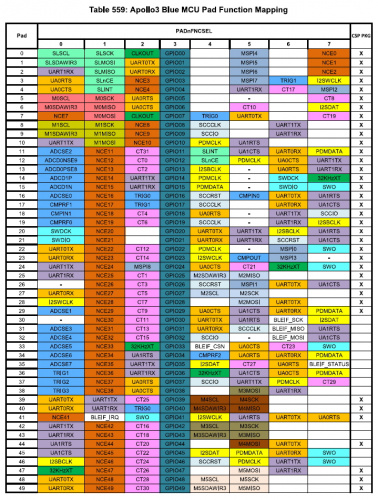
Pad map of the Apollo3
I now know this table by heart. We wanted to break out all 50 GPIOs if possible, and we tried. But it became obvious, after many puzzling attempts, that a few balls would have to be left unconnected. But which ones? Only 10 of the 50 pins are ADC capable, so those were seen as most valuable. Next were PWM pins. There are 32 pins on the Apollo3 that are PWM capable, so those were given additional value. There are two UARTs, six I2C and six SPI ports on the Apollo3. The trick is that these peripherals can be assigned to a variety of different pads. And on the outside chance users wanted to use the SecureCard, PDM or I2S capabilities of the IC, we wanted to be sure to break out those pads and make the maximum number of flexible pins available.
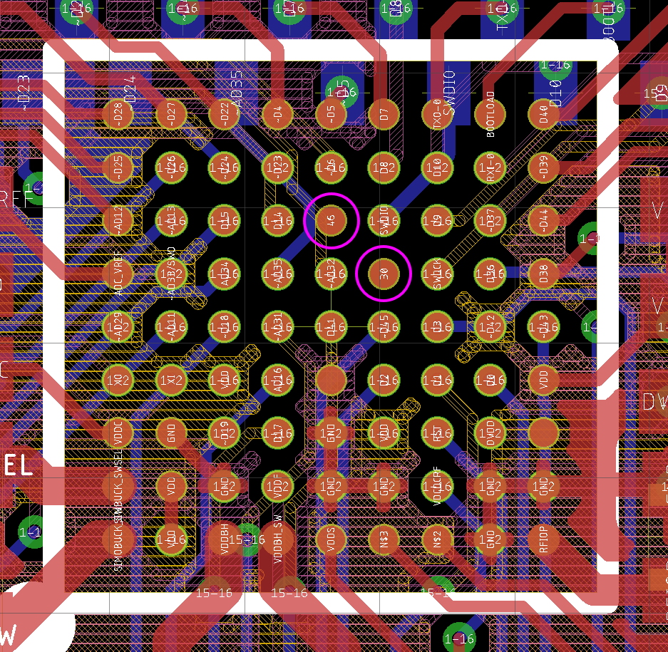
Bon voyage 30 and 46!
A few days of pad valuations and test routing ensued. In the end we had to say goodbye to pads 30 and 46. While 30 has PWM, it became nearly mechanically impossible to break out this inner ball without additional PCB layers. Pad 46 was lovely, but just didn’t have enough peripherals to make it worth going to a six-layer board to break it out.
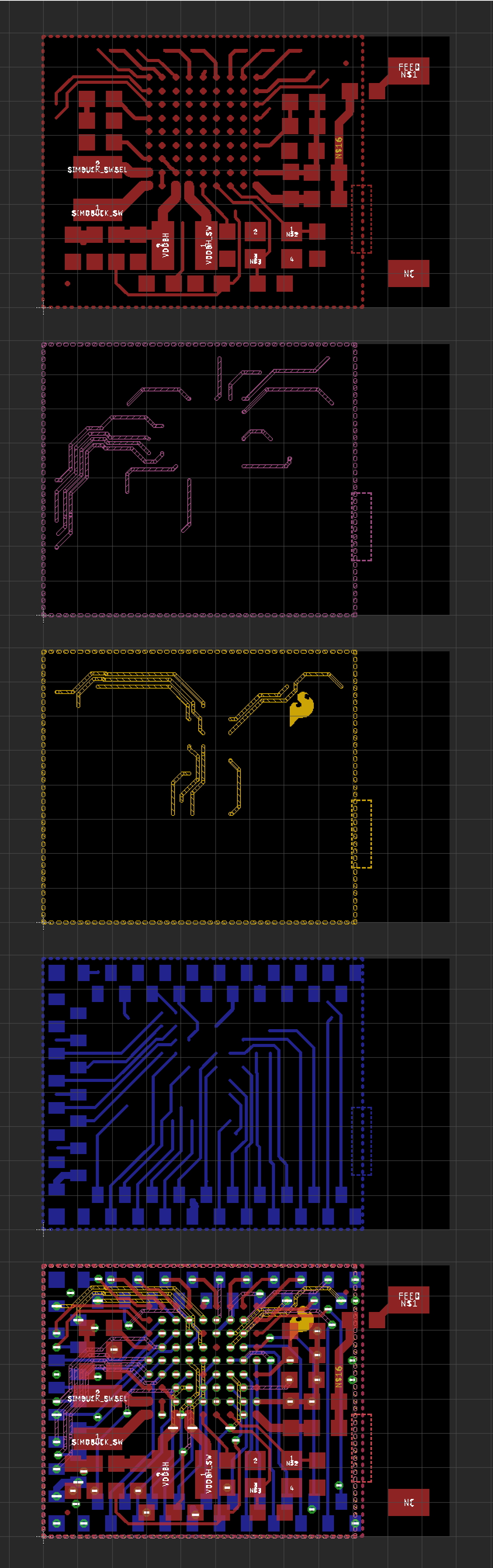
Here are the four layers that make up the Artemis. It looks so simple, but took multiple rounds of protos (remember those long leads times?) and quite a bit of work to get to this stage. But as the first modules began to run "Hello world" blink programs, we started to get very excited at SparkFun. This can be done!
Grouping of Pads
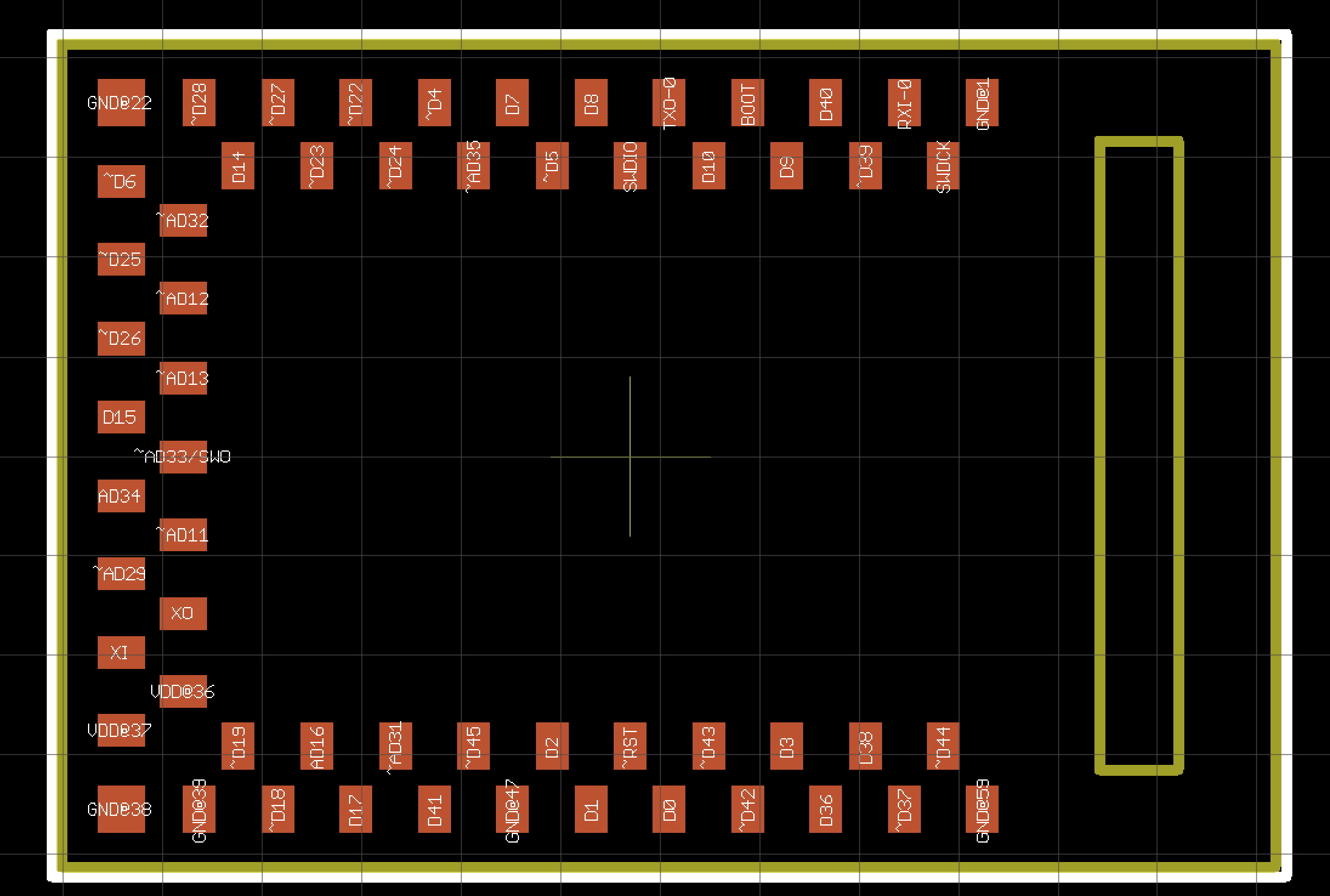
Names of pads on Artemis
If you look closely at the pads on the Artemis, you’ll notice that the pad names seem randomly placed: pad D42 is next to D3, is next to D36, etc. This pains my soul. I really wanted to arrange the pads in sequential order - this would make it easier for the user to navigate the routing of peripherals - but in the end it became untenable. We arranged the pads in the order that made routing most possible. If you’ve ever wondered why a given module has what looks to be completely random pin arrangements, this is why: keeping logical arrangement of pins often gives way to keeping size down.
BOM Beating
Original Artemis Engineering version that shipped without RF shield
As the Artemis design was coming together, every component on the board was reviewed and vetted for cost and supply chain concerns. It was clear that we would be competing in an already cluttered space of WiFi (thanks ESP8266!) and various Bluetooth modules. The race to the bottom has been going on for years, so we would need to keep our overall BOM costs as low as possible to stay competitive in the market. The Apollo3 has a large number of advantages over WiFi and regular, higher-power Bluetooth modules, but we had to be careful picking out the various components.
Finding a super low cost component is obvious, but if you can’t get that part for 10 months then who cares about cost? And you’ve heard that saying, "penny wise but pound foolish," we experience this all the time with suppliers who either disappear or required 17 steps before they will ship an order. Be careful trying to reduce the cost of a button by $0.02; you may end up adding $0.20 when you factor in the overhead of a crummy supplier.
Additionally, once a device has been tested and certified it is a Herculean task to change out a component along the RF path (the most sensitive being the antenna). The biggest choice was the RF antenna. We decided to go low cost (but not lowest) with a well known manufacturer that was responsive and seemed to have plenty of stock available from a variety of sources.
With the primary layout complete, we moved on to designing an RF shield that would mate with the module...but that's a story for next time.


Nice write-up. It's always interesting to hear the backstories like this. I've designed an RF module myself and all these design decisions and routes seems familiar. Waiting for the next part. Thanks.
Please feel free to share your own stories and or lessons. We're far from experts.
Regarding the castellated vs buried pads: Why not use both? Have a wide range of castellated pads that could be used for simpler designs not requiring all of the pins, along with buried pads for the more complex designs.
That way bar to entry is lower (Can be hand-soldered) without limiting more complex projects.
Great write-up, Nate!
Both PCB and IC tachnology has improved by leaps and bounds since I first started playing with electronics in the mid-1960s. PCB technology still has a ways to go, but at the rate it's going, by the 2060s I bet it will be using sie and spacing rules tighter than ICs were in the 1960s! ;-)
Congrats on the FCC certification, but if you really want a challenge, try to get FDA approval! Although there are good reasons for a lot of it (e.g., thalidomide, which caused severe birth defects but has had a resurgence as a treatment for certain types of cancer), there are also times when the "flat" application of the rules can be idiotic and amount to "your tax dollars hard at work scr*wing you over". (BTW, I've never actually been through that successfully. The projects got dropped because of the potential costs of FDA approval for a products with a total-sales prospect was a fraction of the cost.)
Haha, the thalidomide information and FDA approval stuff just reminded me about Prop 65. :P
FCC certification has probably changed a lot from the time of this anecdote so keep that in mind. A "friend" who designed add-on boards for Toshiba laptops in the late 80's had to take them to a lab to obtain certification. To keep it short, he noted that the lab-technoid barely had the skills to run the test, RF-wise. Plus, the rules then stated that testing an after market product for laptops, ALL of the connectors on the laptop had to have cables attached. Since the cables were not terminated, they were hella radiators.
First attempt: failure. The technoid showed him where high freq 'stuff' was showing up on the spectrum analyzer. Knowing what was going on, he said "hold on a moment; I think one or two of the connectors might not be plugged in all the way. Let me go check them".
He walked out into the an-echoic chamber with a pocket full of clamp-on ferrite toroids and deftly snapped them on to the various cables plugged into the laptop. Voila! (or as often seen on the net: viola!) "Run the scan again Sam!" This time all was quiet and the unit passed.
Am I advocating cheating? No, of course not. I would never stoop to such a level.
That was some very creative and darn near ingenious engineering to pull that off. Great job!
With the hidden pads, does the breakout board also reflow again when soldered to the target board?
Regardless of hidden or castellated pins, the module will heat up considerably. The trick is that the Artemis was already reflowed once to be manufactured and the flux was removed during the first process. The second time a module is heated up in the reflow oven the module will approach a molten solder phase but it won't quite make it. Even if the Artemis components do achieve reflow temperatures, molten solder has very high surface tension and will hold the components on Artemis in place.
Another Eagle "trick" is to set the color for vias to BLACK. That way, the vias take the color of the layer they are on, instead of always being green. They will also not appear unless the layer they are on is enabled for display. I have a 12-layer blind and buried via board that would be indecipherable if not for this "trick".
Also, @OldFar-SeeingArt, ...(or as often seen on the net: walla!)
Hey great write up! Curious if you guys did a title page with notes listing planarized vias impedance etc to your supplier since these aren't "typically" processes. If you do would that be something you can show on this thread? I know that for me being introduced to that concept earlier on woulda helped me immensely as I do notes all the time now in my career.